

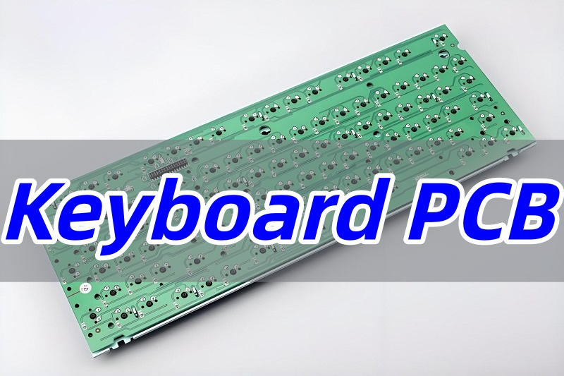
The keyboard PCB is the central nervous system of any input device. This guide provides a professional overview of keyboard PCBs, focusing on the key considerations for bringing a successful product to market.
Developing a new keyboard product presents significant challenges beyond personal preference. Are you facing these critical business hurdles?
- Technical Complexity: Integrating advanced features like Bluetooth connectivity or unique layouts requires specialized firmware and hardware expertise that may not exist in-house.
- Supply Chain Reliability: Sourcing consistent, high-quality components and PCB fabrication, especially during market fluctuations, can jeopardize production timelines.
- Cost-Effectiveness for Low/Medium Volumes: Achieving competitive per-unit costs without the economies of scale of mass production is a constant battle.
- Design for Manufacturability (DFM): A prototype that works on a bench may fail in assembly due to design oversights, leading to costly re-spins and delays.
- Quality Consistency: Ensuring every unit in a production run meets the same performance and reliability standards is a formidable quality control task.
Navigating these challenges requires a manufacturing partner, not just a supplier. The solution lies in selecting a PCB expert who can provide:
- Deep Engineering Support: A partner that offers Keyboard PCB design review and can troubleshoot complex issues from schematic to finished board.
- Robust Supply Chain Management: A manufacturer with established material sourcing channels to mitigate risk and ensure component availability.
- Flexible Production Scaling: A vendor that efficiently handles both prototype quantities and medium-scale production runs without exorbitant costs.
- Proactive DFM Analysis: A team that analyzes your design files upfront to identify and correct potential manufacturing defects before they become expensive problems.
- Rigorous Quality Assurance: A commitment to comprehensive testing protocols, such as Keyboard PCB tester routines, to guarantee consistent performance across the entire batch.
At EBest Circuit (Best Technology), we specialize in being that solution. We are a professional PCB manufacturer focused on serving businesses and innovators. Our core expertise lies in transforming complex designs into reliable, high-yield products. We understand the pressures of product development, and we build our services—from engineering support to flexible production—to meet them. Pls feel free to share your custom keyboard PCB request to us via sales@bestpcbs.com at any moment.
Keyboard PCB Meaning
At its core, a keyboard PCB is the engineered substrate that hosts the electrical pathways connecting all key switches to a microcontroller. It is the fundamental component that translates a physical press into a digital command.
What is the keyboard circuit board called? The accurate term is Printed Circuit Board Assembly (PCBA) for a fully populated board, but within the industry, it is universally referred to as a keyboard PCB.
For product developers, the PCB is not a commodity; it is a critical piece of intellectual property. Its design defines the keyboard’s matrix, which dictates the scanning methodology for key detection. It determines the physical layout, the support for additional features like LEDs, and the overall electrical robustness of the device. Choosing the right base keyboard circuit board is the first step in defining a product’s bill of materials (BOM), cost, and performance.
What Are the Keyboard PCB Features?
Selecting a keyboard PCB involves specifying a set of features that align with your product requirements. These decisions impact user experience, manufacturing complexity, and cost.
- Layout and Form Factor: This is a primary product differentiator. Common standards include the 60% keyboard PCB, 65% keyboard PCB, and the commercially popular 75% keyboard PCB. The choice between a Windows keyboard PCB and a Mac keyboard PCB may involve keycap legend and firmware-level functional key mapping.
- Hot-Swap Capability: A hot swappable keyboard PCB is a significant feature for certain market segments. It allows end-users to change switches without soldering. From a manufacturing standpoint, this requires the inclusion of dedicated sockets (e.g., Kailh Hotswap Sockets), which adds to the BOM cost but enhances the product’s appeal for customization.
- Connectivity Architecture: The decision between a wired keyboard PCB and a Bluetooth keyboard PCB is fundamental. A wired design is simpler and more cost-effective. A wireless design requires RF expertise, certification (FCC/CE), and power management for batteries, significantly increasing complexity.
- Switch Technology: While most custom projects use mechanical switches, understanding alternatives is key. For example, a Hall effect keyboard PCB uses magnetic field sensing for analog input and potentially longer life, representing a premium feature.
- Additional Features: Support for RGB backlighting on a backlit keyboard PCB requires dedicated LED circuits and firmware control. Keyboard PCB plate compatibility must be designed into the mounting hole positions.
What Are the Keyboard PCB Types?
Professionals categorize keyboard PCBs by both their switching technology and their layout size, as these define the product’s market positioning.
Based on the switching mechanism, the four primary types are:
- Mechanical Keyboard PCB: The standard for high-performance and custom keyboards. Each key is an independent switch, offering superior tactile feedback, longevity, and consistency. Most gaming keyboard PCB designs are mechanical.
- Membrane PCB: The dominant technology for cost-sensitive and office keyboards. They use a layered plastic membrane and are typically not user-serviceable. The dislike for membrane keyboards among professionals stems from their mushy feel, lower lifespan, and lack of reparability compared to mechanical switches.
- Scissor-Switch PCB: Common in laptops and low-profile keyboards. They are a type of membrane keyboard but with a scissor mechanism for stability, offering a short key travel.
- Capacitive PCB: These high-end boards, like Topre switches, detect key presses through capacitance changes. They are known for a smooth, quiet feel but come at a premium cost.
Based on layout size, the common commercial types are:
- 100% / Full-size PCB: Includes alphanumeric keys, navigation cluster, and number pad.
- Tenkeyless (TKL) PCB: Removes the number pad for a more compact footprint.
- 75% keyboard PCB: A bestseller because it offers a highly compact layout while retaining the function row, providing an excellent balance of size and utility.
- 65% keyboard PCB: Further reduces size by removing the function row but keeping arrow keys.
- Specialized Layouts: This includes numeric keypads keyboard PCB, split keyboard PCB for ergonomics, and mini keyboard PCB for macro functions.
Does Keyboard PCB Affect Sound?
Yes, significantly. For a product developer, the acoustic signature is a feature that can be engineered.
The PCB contributes to the sound profile through its physical properties and integration:
- Mounting Method: How the PCB is secured in the case (gasket mount, tray mount, top mount) dramatically affects sound damping and vibration transmission. A gasket-mounted board produces a softer, more muted sound compared to a rigidly tray-mounted one.
- PCB Rigidity: A thicker, multi-layer PCB (e.g., 1.6mm vs 1.2mm) is less prone to flex and vibration, resulting in a more consistent and solid sound across the board.
- Design for Acoustic Control: A professional design will include space and mounting points for dampening materials (foam, silicone) between the PCB and the case to eliminate cavity resonance and create a more premium acoustic experience.
How to Do Keyboard PCB Design?
The Keyboard PCB design process is a multi-stage engineering discipline.
- Requirements Specification: Define the product: layout, features (hot-swap, RGB), connectivity, and target cost.
- Schematic Capture: Using an EDA tool (e.g., KiCad, Altium), create the Keyboard PCB schematic. This diagram defines the electrical connections between the MCU, switches, diodes, LEDs, and connectors.
- PCB Layout: This is the most critical phase. It involves component placement and routing the traces according to the keyboard PCB matrix. Care must be taken to avoid signal interference, especially in wireless designs. The layout must adhere to Design for Manufacturability (DFM) rules.
- Firmware Development: The PCB is useless without firmware to scan the matrix and communicate with the host computer. This often involves programming a microcontroller like an RP2040 or an ARM-based chip.
- Prototyping and Validation: Order prototype PCBs, assemble them, and conduct rigorous testing. This includes electrical tests, functional tests, and longevity stress tests.
Where to Get the Custom Keyboard PCB?
Sourcing a custom PCB is not just about finding a fabricator; it’s about partnering with an expert who ensures your product’s success. While generic online PCB services exist for simple boards, complex projects require a specialized manufacturer.
EBest Circuit (Best Technology) is your ideal partner for custom keyboard PCB manufacturing. We go beyond simple fabrication to provide integrated support throughout your product development cycle.
Our core advantages include:
- Expert Design for Manufacturability (DFM) Review: Before production begins, our engineering team conducts a thorough analysis of your design files. We identify potential issues related to solder mask, trace spacing, and assembly that could impact yield, saving you from costly revisions.
- Support for Complex Projects: We have extensive experience with advanced requirements, including Bluetooth keyboard PCB designs requiring impedance control, hall effect keyboard PCB with sensitive analog components, and intricate layouts like split keyboard PCB and Corne keyboard PCB.
- High-Quality Materials and Finishes: We don’t compromise on materials. We use high-Tg FR-4 substrates and offer premium finishes like ENIG (Immersion Gold) for excellent flatness and solderability, which is critical for hot swappable keyboard PCB designs and fine-pitch components.
- Comprehensive In-House Capabilities: From precise keyboard PCB fabrication to component sourcing and assembly, we manage the entire process under one roof. This gives us complete control over quality and timelines.
- Flexible and Responsive Service: We specialize in supporting projects from the initial prototype stage through to small and medium-volume production runs. We provide clear communication and adapt to your specific needs.
Case of Making PCB for Keyboard at EBest Circuit (Best Technology)
A startup company designed an ergonomic mechanical keyboard PCB with excellent electrical performance but faced several manufacturability (DFM) challenges: hot-swap socket pad designs prone to cold joints, USB-C component sourcing risks, and high demands for PCB mechanical strength and aesthetics.
Our Solution & Process Capability Application
- Material Selection & Structural Optimization
- High-Tg FR4 material (KB6167, Tg>170°C) was selected to ensure long-term resistance to bending deformation while supporting 10-layer stack-up (originally 6-layer) for complex signal routing.
- Laser microvias (0.1mm) and mechanical buried vias (0.15mm) enabled high-density interconnects, reducing PCB size for a slimmer keyboard design.
- Precision Circuit & Pad Optimization
- Hot-swap socket pads were reinforced with 3oz outer-layer copper (3/3mil trace/space) for mechanical durability, paired with 4mil solder mask dams (LPI) to prevent solder bridging.
- ENIG (3-8μm Ni, 0.025-0.125μm Au) was applied to enhance USB-C connector durability, with ±1mil NPTH hole tolerance ensuring precise alignment.
- Supply Chain & Surface Finish Innovation
- Matte black solder mask (KSM-6189 KM01) with white legend improved aesthetics while meeting backlight visibility requirements.
- Immersion tin (0.8-1.5μm) replaced HASL to prevent oxidation during repeated hot-swap socket soldering.
- Advanced Process Support
- 20oz outer copper (60/80mil trace/space) strengthened current-carrying capacity for high-load areas like the spacebar.
- CTI600-rated material ensured insulation reliability in humid environments, aligning with spill-resistant design needs.
Industry Applications
This case highlights our expertise in consumer electronics PCB manufacturing:
- High-density interconnects: Ideal for TWS earbuds, smartwatches, and miniaturized devices.
- High-reliability materials: Suitable for industrial controls and automotive electronics in extreme conditions.
- Custom aesthetics: Supports personalized designs for gaming peripherals and smart home products.
By integrating DFM analysis with advanced process capabilities, we empower clients to transform innovative designs into mass-producible, high-quality PCBs.
In conclusion, the keyboard PCB is the core of your product, defining its functionality, quality, and manufacturability. Understanding its technical aspects—from design and types to acoustic properties—is essential for any successful product launch.
Choosing the right manufacturing partner is the most critical decision in this process. As one of a quick delivery keyboard PCB manufacturers for Prototyping, EBest Circuit (Best Technology) provides the engineering expertise, quality assurance, and flexible production services necessary to transform your custom keyboard design from a concept into a reliable, market-ready product. Warm welcome to contact our team at sales@bestpcbs.com to discuss your specific requirements and receive a detailed quotation.
Tags: keyboard pcb