

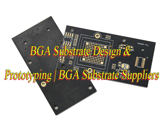
How to design a BGA substrate? Let’s discover structure, materials, features, functions, applications, design guide, production process for BGA substrate.
Are you troubled with these problems?
- Do BGA substrates frequently experience warpage and delamination due to inadequate heat dissipation, compromising product lifespan?
- Are impedance mismatches and signal interference performance bottlenecks during high-speed signal transmission?
- Are prototyping cycles and mass production costs challenging to control under complex design requirements?
As a BGA substrate supplier, EBest Circuit (Best Technology) can provide you service and solutions:
- Thermal Management Expertise: Specialized substrate materials and optimized structural design significantly improve heat dissipation and mechanical strength for long-term reliability.
- Signal Integrity Assurance: Precise process control and simulation enable superior impedance matching and low crosstalk, meeting high-frequency application needs.
- Efficient Production Support: End-to-end services from design to manufacturing reduce lead times, optimize costs, and ensure stable supply for scalable production.
Welcome to contact us if you have any inquiry for BGA substrates: sales@bestpcbs.com.
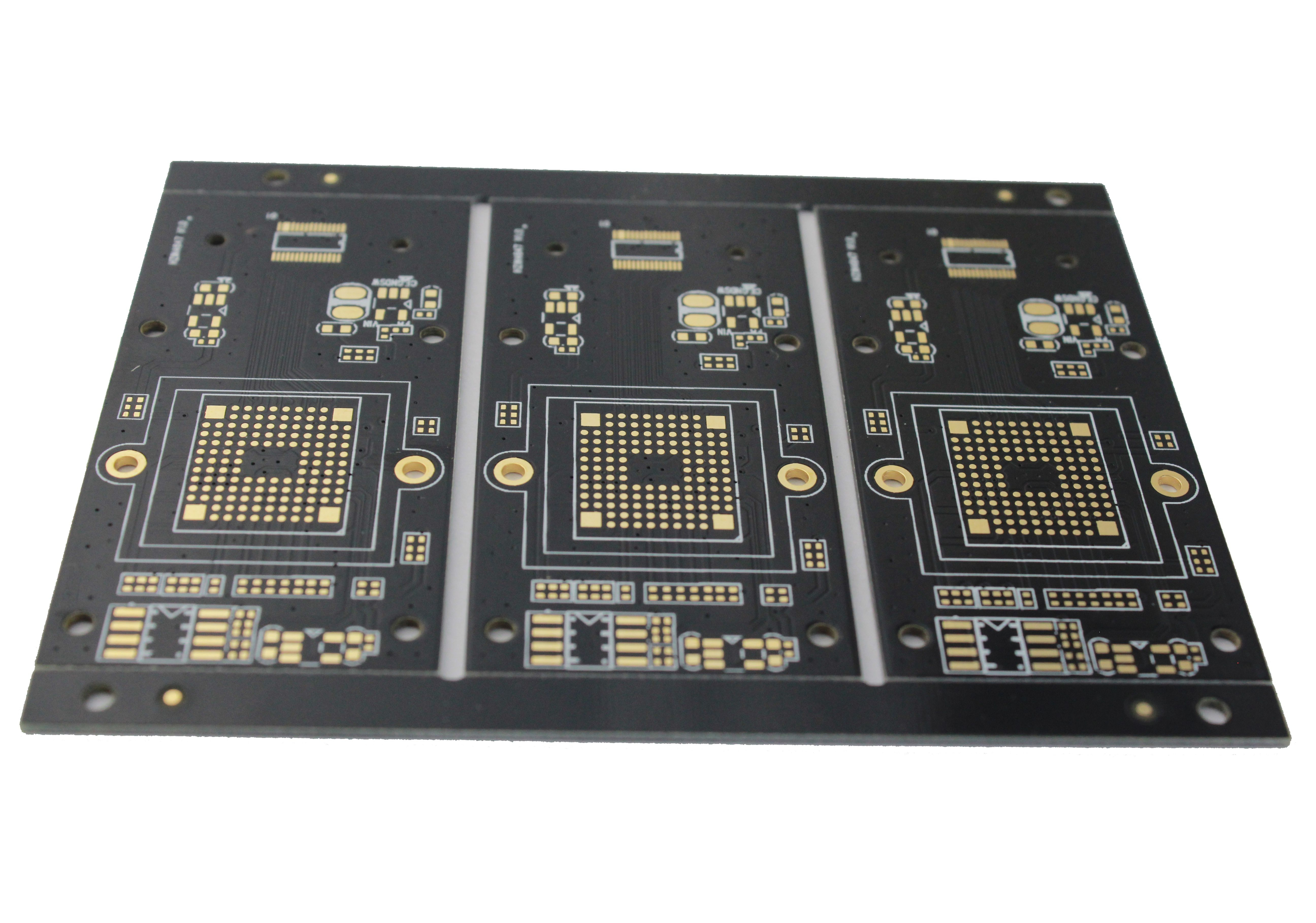
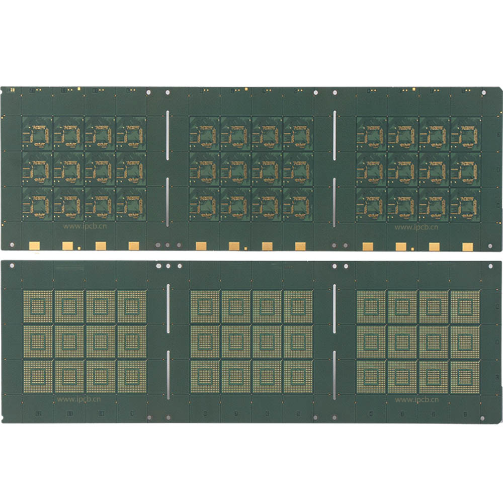
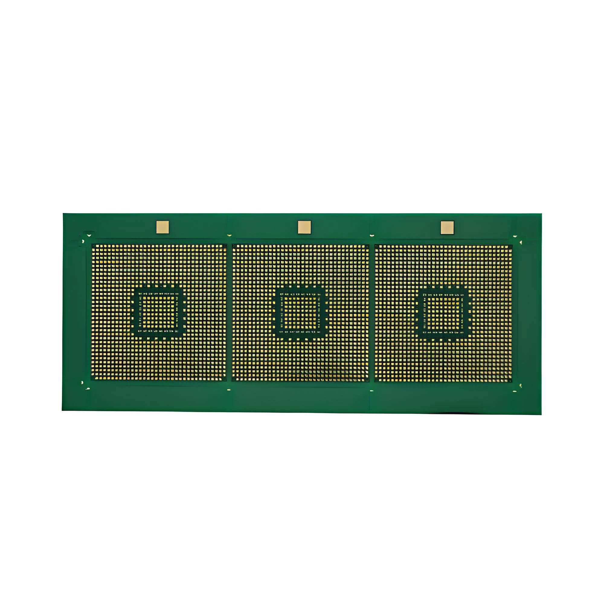
What Is BGA Substrate?
A BGA substrate (ball grid array substrate) is a core component in integrated circuit (IC) BGA packaging and is a multi-layer precision circuit board. Its primary function is to carry the bare chip die. High-density internal interconnects (line width/line spacing can reach micrometers) connect the chip’s tiny electrical contacts to the solder ball array at the bottom of the package, providing electrical connectivity, mechanical support, and heat dissipation between the chip and the external circuit board.
What Is Structure of BGA Substrate?
| Level | Function | Materials |
| Chip Connection Layer | Bonding chips via solder balls/bumps | Copper Pillar, Micro Solder Balls |
| Routing Layer | Signal transmission & power distribution | Copper Traces (Line Width ≤10μm) |
| Dielectric Layer | Insulation & interlayer isolation | ABF Resin, BT Resin, Ceramic |
| Solder Ball Array | Connecting PCB boards | SAC305 Solder (Sn96.5Ag3Cu0.5) |
What Are Materials Used for BGA Substrates?
Substrate Core Materials
- Organic Resin Substrates (e.g., FR-4): The most common low-cost option, composed of glass-fiber reinforced epoxy resin. It offers good mechanical strength and electrical performance but has a relatively high coefficient of thermal expansion (CTE) of approximately 15-18 ppm/°C, which may induce stress during thermal cycling
- Ceramic Substrates (Al₂O₃/AlN/SiC): Al₂O₃ (aluminum oxide) is cost-effective with moderate thermal conductivity (20-30 W/m·K). AlN (aluminum nitride) provides high thermal conductivity (170-200 W/m·K) but at a premium price. SiC (silicon carbide) combines high thermal conductivity with low CTE, making it suitable for high-frequency applications.
- Metal Substrates (Aluminum/Copper): Aluminum substrates are often anodized to form an insulating layer, offering excellent heat dissipation (200-250 W/m·K) at a lower cost than ceramics. Copper substrates deliver superior thermal conductivity (400 W/m·K) but come with higher weight and cost.
Conductive and Interface Materials
- Copper Traces: Employ 18-35μm electrolytic/rolled copper foil. For high-frequency applications, surface roughening is applied to minimize signal loss.
- Surface Finishes: ENIG (electroless nickel immersion gold) is widely used, featuring a 3-5μm nickel layer and 0.05-0.1μm gold layer. ENEPIG (electroless nickel electroless palladium immersion gold) provides enhanced solder joint reliability.
- Solder Alloys: Under lead-free trends, Sn-Ag-Cu (e.g., SAC305) alloys dominate, with melting points of 217-220°C. Silver content influences mechanical strength and ductility.
Auxiliary Materials
- Dielectric Layers: High-performance substrates utilize modified epoxy or polyimide, with dielectric constants of 3.5-4.5 (at 1MHz) and dissipation factors of 0.01-0.02.
- Solder Mask: Liquid photoimageable solder mask (LPI) achieves resolutions up to 25μm and withstands temperatures exceeding 280°C for 10 seconds.
What Are Features of BGA Substrate?
Features of BGA Substrate:
- High-Density Interconnect Structure: Utilizes HDI process with line width/spacing down to 10μm/10μm and microvia diameter ≤50μm, enabling fan-out routing for thousands of chip I/O interfaces.
- Multi-Layer Stack Structure: Typical layer count of 4-12 layers including signal, power, and ground planes, supporting complex circuit layout and impedance control.
- Low-Dielectric Materials: Employs ABF/BT resin dielectrics (Dk≤3.8, Df≤0.008) to ensure high-speed signal integrity.
- Precision Thermal Management: Thermal conductivity ≥0.5W/(m·K) with embedded copper structures, meeting 300W+ chip power dissipation requirements.
- Ultra-Low Flatness Tolerance: Warpage control <0.1% (<0.1mm deformation for 100mm×100mm substrate), ensuring chip mounting yield. High-Reliability Connections: Withstands >1000 thermal cycles (-55°C~125°C) and >1500G mechanical shock, guaranteeing 15+ years of service life.
- Specialized Surface Finishes: Pads use ENIG/ENEPIG processes with solder ball bonding strength >10N/mm².
- CTE Matching Optimization: CTE adjusted to 14ppm/°C (XY-axis) to match chips, Z-axis CTE ≤70ppm/°C reducing stress cracking risk.
What Are Functions of BGA Substrate?
Functions of BGA Substrate:
- Electrical Interconnection: Serves as a critical interposer between chip (Die) and PCB, providing precision conductive pathways (traces, vias, pads) for electrical signal and power transmission.
- Mechanical Support: Offers robust physical support and mounting platform for fragile silicon chips, protecting them from mechanical stress and deformation.
- Thermal Channel: Substrate designs (especially with metal layers/thermal vias) conduct and dissipate heat to PCB/external heat sinks during chip operation, preventing thermal failure.
- Physical Protection: Provides isolation/protection for chip underside and internal interconnects (e.g., solder balls, wires), reducing environmental erosion from moisture/contaminants.
- Solder Interface: Bottom arrayed solder pads form reliable soldering interfaces, enabling high-density, low-inductance electrical/mechanical connections to PCB via solder balls.
What Are Applications of BGA Substrate?
Applications of BGA Substrate:
- Consumer Electronics: CPU/GPU/memory packaging for smartphones/tablets (e.g., Huawei Watch GT4’s BGA chip enabling ECG functionality) with high-density interconnect & miniaturized design for HD video/complex graphics processing.
- Computer Hardware: CPUs/GPUs/chipsets on PC motherboards, server storage controllers, and laptop CPUs/GPUs using BGA for efficient thermal management & high pin density, ensuring stable operation.
- Automotive Electronics: Engine control modules, safety systems (ABS/ESP), and autonomous driving radar modules (e.g., Tesla Model S’s BMS) adapted to high-temp/vibration environments for improved fuel efficiency/reliability.
- Medical Devices: Pacemakers, glucometers, ECG machines, and medical imaging modules (e.g., rice-grain-sized implantable glucometers) for high-precision signal transmission/long-term use.
- Aerospace: Satellite communication modules and Mars rover navigation chips (e.g., NASA’s Perseverance using CBGA) with radiation-hardened design for -55°C~125°C operation in extreme environments.
- Industrial Control: Microprocessors in industrial automation/instrumentation adapted to harsh conditions (high temp/humidity/vibration) with strong anti-interference capability for reliable operation.
- Telecom Equipment: 5G base station RF chips and router/switch modules using BGA for low-inductance, high-speed signal transmission to enhance communication quality/data efficiency.
- Wearables: Flexible BGA-packaged heart rate monitoring chips (0.1mm thickness) for smartwatches with 7-day battery life, supporting real-time health monitoring.
- Quantum Computing: Cryogenic controllers for quantum computers (e.g., IBM’s BGA-packaged units) achieving 99.99% quantum state fidelity for complex quantum tasks.
How to Design a BGA Substrate?
BGA Substrate Design Guide
1. Requirement & Specification Definition
- Electrical requirements: Count I/O, power/ground, differential pairs, and high-speed signals (e.g., PCIe, DDR, USB); specify single-ended 50Ω/differential 100Ω impedance requirements; analyze power rails’ voltage, current, and ±2-5% ripple tolerance.
- Physical specifications: Determine substrate dimensions/thickness based on chip size and pin count; design ball grid array type (full/peripheral/staggered), pitch (0.4-1.0mm), ball diameter, and height; define PCB connection method and mechanical fixation scheme.
- Environmental requirements: Specify temperature/humidity ranges and reliability standards (e.g., MSL, TC, THB, drop test).
2. Substrate Material Selection
- FR-4: Suitable for low-speed (<1Gbps), low-power scenarios with low cost but poor Dk stability and higher Df.
- Mid-loss materials: Megtron 4/6/7, I-Speed, N4000-13/29SI (Df=0.005-0.010) for 5-16Gbps signals (e.g., PCIe 3.0/4.0).
- Ultra-low loss materials: Megtron 7, Rogers 4350B, Astra (Df≤0.005) for 16Gbps+ high-speed scenarios (e.g., PCIe 5.0/6.0).
- Thermal considerations: Select high-Tg (≥170°C) materials for improved high-temperature stability; match X/Y/Z CTE (silicon ≈2.5ppm/°C, PCB ≈16ppm/°C) to reduce solder joint stress.
- Copper foil selection: VLP/HVLP copper foil recommended for high-frequency applications to reduce skin effect losses.
3. Layer Stackup & Power Design
- Stackup structure: Symmetrical design to prevent warpage; high-speed signal layers sandwiched between GND/PWR planes for impedance control and shielding.
- PDN design: Rational power plane segmentation to avoid split routing; high-frequency decoupling capacitors (0.1μF/0.01μF) placed close to power pins; bulk capacitors (10μF) for mid/low-frequency needs; calculate target impedance via Ztarget=Vripple/Imax and validate via simulation.
4. Signal Integrity Design
- Impedance control: Calculate microstrip/stripline impedance using Polar SI9000; ensure board house process accuracy ±10%.
- Routing rules: Follow 3W rule to minimize crosstalk; use 45° angles/arcs to avoid impedance discontinuities; match lengths for differential pairs/buses (e.g., differential pairs ±5mil, DDR ±25mil).
- Via design: Backdrill to remove stubs or use via-in-pad with filling for high-speed signals; add shielding vias near critical signals for low-inductance return paths.
5. Thermal Management Solutions
- Thermal pathways: Dense thermal vias (8-12mil diameter) under chip hotspots filled with high-thermal-conductivity material; add thick copper layers (e.g., 2oz) internally/backside as thermal spreaders.
- External cooling: Design mounting holes for heatsinks/vapor chambers on the substrate top; use thermal interface materials (silicone grease/pads) between chip and heatsink; for high-power chips, conduct heat to PCB thermal pads via larger solder balls/copper pillars.
6. Pad & Routing Design
- Pad types: NSMD (non-solder mask defined) is commonly used, where solder wraps the copper pad for stronger mechanical bonding; SMD (solder mask defined) prevents pad peeling in ultra-fine-pitch scenarios.
- Escape routing: Calculate routing channels (channels=(Pitch-Ball Diameter)/(Line+Space)); use laser microvias (0.1mm) and HDI stackups (1+N+1/2+N+2) for fine-pitch (≤0.5mm) BGAs; prioritize routing for critical signals like clocks/differential pairs.
7. Manufacturing & Testability
- DRC checks: Set CAD tool rules based on board house capabilities (line width/spacing, hole size, alignment accuracy); focus on BGA area spacing to prevent shorts.
- Marking & testing: Clearly label Pin 1 and test points; reserve edge test points for critical nets (clocks/power); ensure JTAG chain accessibility.
8. Simulation & Validation
- Pre-layout simulation: Use IBIS/AMI models to explore topologies and termination schemes; determine optimal trace lengths/termination resistor positions.
- Post-layout simulation: Extract S-parameter models for SI (eye diagram/jitter/BER), PI (target impedance/SSN), and thermal simulation (junction temperature/hotspots); output Gerber/IPC-356/drill files and assembly instructions (stencil apertures/solder profile).
How to Make a BGA Substrate?
BGA Substrate Production Processes
1. Substrate Material Selection and Adaptation
- Organic resin substrates (FR-4): Preferred for cost-sensitive scenarios, with thickness adapted to design needs (e.g., 1.6mm). Control CTE (15-18ppm/°C) to reduce thermal stress. High-Tg FR-4 (Tg≥170°C) suits lead-free soldering, requiring Td (decomposition temperature) ≥340°C validation.
- Ceramic substrates (Al₂O₃/AlN/SiC): Al₂O₃ offers low cost and 20-30W/mK thermal conductivity; AlN provides 170-200W/mK for high-frequency/high-power applications; SiC combines low expansion (3-4ppm/°C) and high-frequency performance but requires mechanical shock protection due to brittleness.
- Metal substrates (aluminum/copper): Aluminum substrates form insulating layers via anodization, with 200-250W/mK thermal conductivity. Copper substrates deliver 400W/mK but have higher weight and cost, necessitating optimized thermal path design.
- High-performance materials: Ultra-low-loss materials (e.g., Megtron 7, Rogers 4350B, Df≤0.005) for 5G+ high-frequency scenarios. BT resin (Tg 170-220°C) balances cost and performance for multi-layer PCBs.
2. Inner Layer Circuit Production and Pattern Transfer
- Pre-treatment: Chemical cleaning (e.g., SPS acid wash) removes copper surface oil and oxides. Micro-etching (e.g., Na₂S₂O₈ solution) increases surface roughness for improved dry film adhesion.
- Lamination and exposure: LDI (laser direct imaging) exposure machines achieve micron-level precision. Dry film thickness is 1.2-2mil, with exposure energy calibrated to 6-8 light scale levels to avoid over/under exposure.
- Developing and etching: Developing solution (0.85-1.3% Na₂CO₃) removes unexposed dry film. Etching uses CuCl₂ solution at 48-52°C and 1.5-2.2m/min speed to ensure line width/spacing precision (e.g., 3.5/3.5mil for 0.5mm pitch).
- Solder mask production: LPI (liquid photoimageable) solder mask ink achieves 25μm resolution and ≥280°C/10s thermal resistance. Opening dimensions are precisely controlled (solder mask is 0.05-0.1mm smaller than pads).
3. Lamination and Stack-Up Process Control
- Multi-layer stack-up: Inner core boards and prepreg (PP sheets) are alternately stacked and pressed under high temperature/pressure (e.g., 160°C/140min/2.5MPa) to form multi-layer structures, requiring symmetric design to prevent warpage. HDI technology (e.g., 1+N+1 structure) enables blind/buried vias with ≤150μm diameter and 8-12mil target pad diameter.
- Drilling and metallization: Mechanical drilling achieves ±0.05mm precision. Laser drilling (0.1mm diameter) for blind vias. Hole walls are electroplated with ≥150μm copper for interlayer connectivity. Backdrilling removes stubs to minimize signal loss.
- Thermal pressing parameters: Vacuum hot presses control temperature curves. Epoxy resin in prepreg melts and flows under high temperature, with pressure ensuring void-free interlayers. Slow cooling rates reduce internal stress.
4. Electroplating and Surface Treatment Processes
- Copper foil electroplating: “Conformal anode + auxiliary cathode” technology optimizes current distribution, with layer uniformity deviation ≤±10%. CPU socket pads require 4±0.4μm thick gold plating.
- Surface treatment types: ENIG (electroless nickel immersion gold) provides 3-5μm nickel and 0.05-0.1μm gold for improved solder reliability. ENEPIG adds palladium for enhanced corrosion resistance. VLP/HVLP copper foil reduces skin effect losses in high-frequency scenarios.
- Solder ball production: SAC305 (Sn-3.0Ag-0.5Cu) lead-free solder forms balls via precision heating and surface tension, with diameter adapted to design needs (e.g., 0.75mm) and ±0.02mm tolerance.
5. Solder Ball Assembly and Packaging Processes
- Reflow soldering: Nitrogen-environment reflow uses precise temperature curves (preheat 150-180°C/60-90s, peak 217-220°C, cooling ≤4°C/s) to prevent oxidation and voids.
- Encapsulation molding: Epoxy resin molding protects chips, with curing conditions (e.g., 150°C/2h) ensuring hardness and stability. High-power chips use TIMs (thermal interface materials) with ≥5W/mK conductivity to fill chip-heatsink gaps.
- Underfilling: Epoxy resin + filler underfill injected between chip and substrate enhances mechanical strength and reduces thermal stress cracking after curing.
6. Testing and Quality Inspection Methods
- X-ray inspection: 2D X-ray checks solder joint morphology; 3D X-ray tomography analyzes internal voids (e.g., bubble diameter ≤30% for Class 3 standards). Ultrasonic testing identifies delamination defects.
- Thermal imaging analysis: Infrared cameras measure BGA component temperature distribution, with hotspots below 80% of material glass transition temperature. Thermal cycling tests (-40°C~125°C/1000 cycles) validate solder joint reliability.
- Electrical testing: ICT (in-circuit testing) detects opens/shorts; flying probe tests verify JTAG logic connectivity. Impedance control is validated via TDR (time-domain reflectometry) for single-ended 50Ω/differential 100Ω.
- Visual inspection: AOI (automated optical inspection) checks pad/solder mask defects. Microscopy examines solder ball coplanarity (deviation ≤0.1mm) for PCB pad alignment precision.
7. Process Optimization and Reliability Enhancement
- Environmental adaptability: MSL (moisture sensitivity level) testing ensures humidity resistance. HAST (highly accelerated stress testing) validates long-term reliability. Automotive-grade products meet AEC-Q100 certification for -40°C~150°C operating ranges.
- Thermal management: Dense thermal via arrays (8-12mil diameter) beneath chip hotspots filled with high-conductivity materials (e.g., copper paste). Thick copper layers (2oz) on substrate backside act as thermal spreaders for lateral heat dissipation.
- Mechanical strength: NSMD (non-solder mask defined) pads wrap solder around copper for stronger bonding. SMD (solder mask defined) prevents pad peeling in ultra-fine-pitch scenarios.
Why Choose EBest Circuit (Best Technology) as BGA Substrate Suppliers?
Reasons why choose us as BGA substrate supplier:
- Free DFM Analysis Directly Reduces Development Costs: Provide free design for manufacturability analysis to identify production risks early minimize redesign costs ensure first-pass design success and save time and capital.
- Ultra-High Precision Manufacturing Process: Ensures Signal Integrity Utilize advanced laser drilling and electroplating technologies to achieve line width/spacing of ≤75μm ensuring stable signal integrity and enhanced performance of end products.
- Rapid Response Delivery System: Meets Urgent Project Needs Implement 24/7 online response mechanism deliver standard prototypes in 7 days and fulfill mass production orders within 15 days accelerating time-to-market.
- Customizable Material Solutions: Offer multi-material options including FR4 high-speed substrates and ceramic baseplates optimized for specific application scenarios to balance cost and performance requirements.
- Comprehensive Quality Control: Ensures Consistent Batch Quality Implement 16 strict inspection stages from raw material testing to final product validation maintain defect rates below 50ppm and support third-party audit verification.
- Intelligent Supply Chain Management: Prevents Production Delays Establish strategic inventory agreements with upstream copper foil and resin suppliers to ensure stable key material supply and avoid production halts due to material shortages.
- Professional Technical Support Team: Resolves Technical Challenges Deploy engineers with over 10 years of BGA substrate design experience to provide full-process technical support from stack-up design to signal integrity simulation addressing client pain points.
- Green Manufacturing Complies with Global Environmental Standards: Obtain ISO 14001 certification adopt lead-free processes and wastewater recycling systems meet RoHS/REACH and other international environmental regulations facilitating export compliance for client products.
Welcome to contact us if you have any request for BGA substrate: sales@bestpcbs.com.