

High speed board design plays a crucial role in modern electronics, from communication devices to automotive systems. This blog highlights the contents about the meaning, significance, and key aspects of high speed board design, critical performance factors, practical improvement strategies, software tools, cost-quality balance, and manufacturing considerations.
Are you struggling with these common pain points?
- Long design schedule and varying difficulty of design?
- The prominent problem of signal completeness?
- Main challenge of manufacturing and process?
- Increased mismatch of design tool and process?
- Great cost of inspection and verification?
With these comprehensive solutions, even the toughest difficulties can be tackled.
- Boost the design process and tools.
- Provide material and process optimization.
- Offer technical support and a high speed board design tutorial.
- Make a modular design and standardization.
- Elevate layout and Routing Strategies.
As a high speed PCB manufacturer, EBest Circuit (Best Technology) provides services varying from high speed board design guidelines, prototyping, mass production, PCBA, and box build. Our product category is not just high speed boards, but also high frequency laminate PCB boards, HDI PCBs, thermally conductive PCBs, robotic aluminum substrate PCBs, and others. These products are best-selling in America, Australia, Israel, Germany, and other countries in the first half of 2025. Warm welcome to send us any technical project to proceed at sales@bestpcbs.com, and we are looking forward to having a close business interaction with you.
What is a High Speed Board Design?
High speed board design refers to PCB layouts intended for circuits with signal frequencies exceeding 100 MHz or signal propagation times below 1 nanosecond (ns). The core objective is to ensure signal integrity (SI), power integrity (PI), and electromagnetic compatibility (EMC). Compared to standard PCB design, high-speed design must address more complex signal transmission issues, such as reflections, crosstalk, and delays. Therefore, it relies on specialized routing strategies, impedance control, and differential pair techniques.
Fundamental Concepts
Signal Integrity
High-speed PCBs require impedance matching (for example, maintaining transmission line impedance at 50 Ω or 100 Ω), avoiding right-angle traces, and using length-matched routing to minimize signal distortion. In contrast, standard PCBs usually operate at lower speeds and rarely require such strict signal integrity considerations.
Material Selection
High-speed PCBs use substrates with low dielectric constant (Dk) and low dielectric loss factor (Df), such as PTFE or Rogers materials, to reduce signal attenuation. Standard PCBs, on the other hand, typically use more cost-effective FR-4 materials.
Power and Thermal Management
High-speed designs require optimized power plane layouts and additional decoupling capacitors to suppress voltage fluctuations. Since high-speed operation generates more heat, thermal management must be enhanced through heat-spreading layers or thermally conductive materials like thermal adhesives.
Key Differences from Standard PCBs
- Design Complexity: High-speed PCBs need signal integrity simulation and impedance control, while standard PCBs only require basic electrical connectivity.
- Cost: High-speed PCBs are significantly more expensive due to advanced materials, processes (such as blind/buried vias), and rigorous testing requirements.
- Applications: High-speed PCBs are used in high-frequency fields such as communications and radar, whereas standard PCBs are mainly applied in low-speed consumer electronics.
From the comparison above, it is clear that high-speed PCB design is crucial for achieving high performance in electronic devices. Its technical requirements and costs are considerably higher than those for standard PCB design.
Why High Speed Board Design Matters in Modern Electronics?
1. Safeguarding Signal Integrity for Greater System Reliability
High-speed signals such as 5G, SerDes, and DDR5 are easily affected by reflection, crosstalk, and delay during transmission, which may lead to bit errors or even system crashes. Standard PCB materials tend to attenuate high-frequency harmonics more severely, meaning signals cannot “travel far.” It is similar to a fuel-hungry car that runs out of gas before reaching its destination. High-speed materials, with lower Df values, minimize signal loss and maintain higher bandwidth and margin over the same trace length. With impedance matching, proper termination, and strict length control of differential pairs (error <5mil), signal integrity is preserved and system stability is greatly improved.
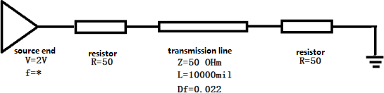
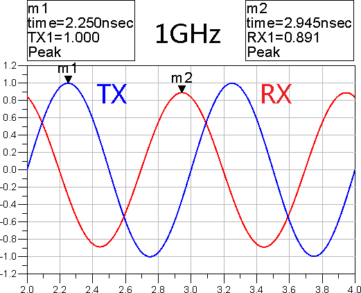
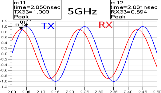
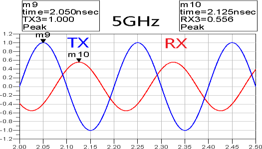
To make this concept more intuitive, a simple simulation circuit is provided to compare the signal performance of a 10-inch trace on Standard Loss material versus Very Low Loss material. By applying sine waves of different frequencies, the impact of dielectric loss on signal transmission becomes clear.
10-inch trace on Standard Loss material
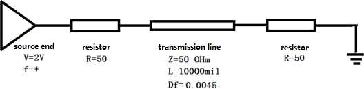
10-inch trace on Very Low Loss material
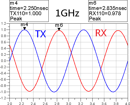
1GHz sine wave comparison
5GHz sine wave comparison
25GHz sine wave comparison
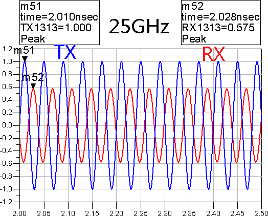
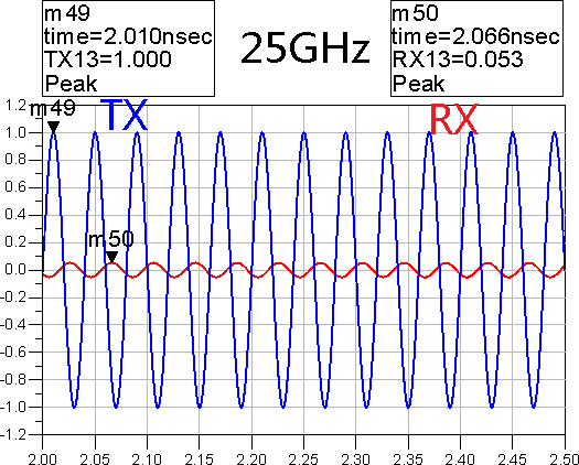
From the results, it is evident that standard materials show much greater attenuation at higher frequencies. At 25GHz, the waveform is almost completely degraded, while low-loss materials retain higher amplitude and sharper edges. Since digital signals are composed of multiple frequency harmonics, the attenuation of high-frequency components leads to edge degradation, reduced amplitude, and lower bandwidth. High-speed laminates reduce transmission loss per unit length, enabling longer traces under the same loss requirement or higher bandwidth under the same trace length.
2. Meeting the Growing Demand for High Frequency and High Density
Modern applications such as millimeter-wave radar, satellite links, and AI processors require PCBs to support GHz-level or even higher frequencies. High-density routing demands finer line width (as small as 3mil) and tighter spacing, along with low-loss materials such as Rogers 4350B to minimize attenuation. Standard laminates act like “gas guzzlers” that cannot sustain long traces, while ultra-low-loss materials function like “fuel-efficient cars,” supporting longer interconnects and higher frequencies. With buried and blind vias, multi-layer interconnections are also made more compact, enabling complex system integration in a limited footprint.
3. Enhancing Power Delivery and Thermal Management
High-speed devices consume more power and generate more heat. Without proper optimization, signals may jitter, and systems may fail. High-speed PCBs focus on robust PDN (Power Distribution Network) design, often using multi-layer stack-ups such as GND-PWR-GND structures combined with decoupling capacitors (10–100nF per chip) to reduce noise. Thicker copper (2oz) and dense thermal vias (0.3mm) improve heat dissipation. Compared to a car that stalls mid-way due to inefficiency, high-speed designs are like performance vehicles—running efficiently, completing the full journey, and maintaining stability.
4. Reducing EMI Risks and Ensuring Regulatory Compliance
High-speed signals radiate more strongly due to their higher frequencies, making them prone to EMI issues. Without proper control, not only does the signal itself degrade, but surrounding devices may also be disturbed. High-speed design employs ground plane segmentation, shielding layers, and the 3W rule (trace spacing ≥ 3 times the trace width) to reduce coupling and radiation. For instance, automotive electronics must meet CISPR 25 standards, while consumer electronics must comply with FCC/CE requirements. Standard laminates, with inconsistent loss characteristics, pose higher EMI risks. In contrast, low-loss laminates with stable dielectric properties combined with optimized layouts help designs pass compliance testing smoothly and avoid costly rework.
5. Driving Miniaturization and Cost Optimization
Beyond performance, high-speed PCB design enables smaller form factors and cost reduction. By optimizing the stack-up (e.g., replacing an 8-layer board with a 6-layer board) and using simulation tools such as HyperLynx and Sigrity, engineers can cut down on unnecessary test iterations. In smartphones, for example, high-speed PCB design allows RF modules and baseband chips to be integrated on a single board, reducing external components and lowering the BOM cost. Just like a fuel-efficient car that runs farther, high-speed design provides more design margin, bringing advantages in both cost and space.
6. Why Businesses Must Prioritize High-Speed PCB Design?
- Technological barrier: Mastering high-speed design skills (e.g., 100Gbps SerDes, DDR5 routing) is the ticket to entering premium markets such as data centers and autonomous driving. Companies without such capabilities find it hard to compete, while those with them gain a key edge.
- Yield control: Poor signal integrity can raise rework costs by more than 30%. By selecting appropriate high-speed materials (from Standard Loss to Ultra Low Loss grades) and optimizing through early-stage simulation, manufacturers can significantly increase yield.
- Faster iteration: High-speed design tools (e.g., Cadence Sigrity, HyperLynx) shorten debugging cycles by nearly 50%, accelerating time-to-market. In today’s race, the companies with “fuel-efficient cars” always reach the finish line first.
To conclude, the importance of high-speed PCB design lies not only in achieving longer and more reliable signal transmission but also in enabling businesses to win in high-end applications and fast-paced markets. From fuel-efficiency analogies to Df-based material classification, from GHz-level communications to automotive compliance, high-speed PCB design has become the backbone of modern electronics. Ignoring it risks reliability and competitiveness; embracing it delivers higher performance, lower risk, and faster innovation.
Critical Factors Affecting High Speed PCB Performance
High speed PCB performance is not determined by a single parameter, but by the synergy between material properties, signal design, power management, and manufacturing precision. Below are the key factors that designers and manufacturers must address:
1. Signal Integrity
Clean signal transmission is the cornerstone of high speed design. Issues such as jitter, overshoot, crosstalk, and reflections can lead to timing errors and data loss. Techniques like impedance matching (50Ω single-ended, 100Ω differential), controlled differential pair routing, and length matching (tolerance <5 mils) are crucial to maintaining accuracy. For dense layouts, 3D simulation tools help minimize crosstalk by ensuring spacing follows the “3W rule.”
2. Material Properties and Loss Control
The choice of PCB laminate has a direct impact on insertion loss at high frequencies. Materials are classified by loss factor (Df), ranging from Standard Loss (0.015–0.020) to Ultra-Low Loss (<0.003). For example, Rogers 4350B or equivalent low-Df substrates are preferred for PCIe 4.0, SerDes, or 100Gbps channels. Additionally, copper foil roughness matters: HVLP copper reduces conductor loss by 12–16% compared to HTE foil, improving signal quality under skin effect conditions.
3. Impedance Control and Interconnect Design
Consistent impedance across transmission paths prevents reflections that degrade performance. Over vias, back-drilling is often applied to remove stubs (e.g., 0.5 mm) that otherwise cause impedance discontinuities. Differential via structures with optimized anti-pad designs (“dog-bone” style) help maintain return paths. These design practices significantly reduce insertion loss and return loss at multi-GHz ranges.
4. Layer Stackup Strategy
A well-planned stackup not only supports impedance stability but also minimizes EMI. High speed boards often adopt symmetrical arrangements such as GND–Signal–PWR–Signal–GND, ensuring solid reference planes. Embedding high-speed traces between planes shields them from external noise. Careful dielectric thickness control (±10% tolerance) keeps impedance consistent, which is vital for signal integrity.
5. Trace Geometry: Width and Spacing
The width, spacing, and uniformity of traces directly affect propagation delay and crosstalk. For example, 3 mil trace/space capability enables dense routing without sacrificing performance. To control coupling, designers follow spacing rules such as ≥3 times the trace width. Consistency is critical—variations in trace width beyond ±10% can cause impedance drift and signal degradation.
6. Power and Ground Plane Design
Stable power delivery and low noise levels are essential for reliable operation. Multi-layer PCBs often use GND–PWR–GND sandwich structures to reduce loop inductance. Decoupling capacitors (10–100 nF per chip) suppress power rail noise, while solid ground planes prevent splits that can generate unwanted EMI. Properly designed return paths are equally important for minimizing ground bounce in high-speed switching.
7. Electromagnetic Compatibility (EMC)
High speed signals are natural sources of EMI. Following the 3W rule, adding guard traces, and using shielding planes help suppress radiation. Automotive systems, for example, must comply with CISPR 25, making EMC-oriented design indispensable. Simulation tools such as HyperLynx can predict EMI hotspots before prototyping, saving costly iterations.
8. Thermal Management and Reliability
High-speed ICs generate more heat, which can impact signal performance and long-term reliability. Thermal vias (0.3 mm drill size) and thicker copper layers (≥2 oz) improve dissipation. Materials like NE-glass fiber cloth also reduce dielectric loss and improve stability at elevated temperatures. Reliability further depends on process control: reflow soldering peaks at 260 °C must not delaminate laminates.
9. Manufacturing Tolerances and Testing
Even a perfect design can fail if manufacturing tolerances are not met. Line width and spacing tolerances of ±10% are typical targets. Advanced test methods such as Time-Domain Reflectometry (TDR) and S-parameter analysis verify insertion loss, return loss, and consistency with simulation models. Strict process control reduces rework and improves yield.
✅ EBest Circuit (Best Technology)’s Approach
At EBest Circuit (Best Technology), we integrate advanced simulation, material selection guidance, and manufacturing expertise to address these challenges holistically. From recommending ultra-low-loss laminates to performing S-parameter validation, our team ensures high speed boards meet both electrical performance and compliance standards. This reduces trial-and-error cycles, shortens time-to-market, and increases end-user competitive edges.
How to Improve High Speed Board Design?
Designing high speed PCBs requires careful consideration of multiple interdependent factors. Beyond simple trace layout, designers must address signal integrity, power distribution, electromagnetic compatibility, and mechanical reliability. Below is a more structured and professional outline for improving high speed board design.
1. Signal Integrity and Trace Management
- Minimize Trace Length: Shorter signal paths reduce propagation delay and signal degradation. Critical high-speed signals should be routed along the most direct paths to avoid unnecessary reflections and jitter.
- Use Differential Pairs: For key signals such as high-speed serial interfaces (USB, PCIe), differential routing helps suppress common-mode noise and improves noise immunity. Differential traces must maintain matched lengths to ensure timing consistency.
- Impedance Control: Maintain consistent impedance across layers. The choice of trace width, spacing, and distance to the reference plane directly affects signal reflections and losses. Tools such as SI simulators or field solvers can verify impedance accuracy before fabrication.
- Crosstalk Mitigation: Increase spacing between adjacent traces, use ground traces or planes as shields, and consider orthogonal routing on adjacent layers to minimize coupling between high-speed lines.
2. Layer Stackup and Plane Design
- Optimize Layer Arrangement: Place signal layers adjacent to reference planes (ground or power) to ensure controlled impedance and reduce EMI. High-speed layers should ideally be sandwiched between planes for shielding.
- Power and Ground Plane Strategy: Avoid “dumbbell-shaped” splits that reduce current-carrying capacity and create hotspots. Use continuous planes wherever possible, and maintain short, wide planes to minimize voltage drops.
- Via and Copper Pour Management: Vias introduce gaps in planes, which can increase impedance and create hotspots. Place vias in a grid to distribute current evenly and reduce localized impedance changes. Copper pours on top layers should be connected to ground at multiple points to prevent forming unintended antennas.
3. Power Integrity and Decoupling
- Decoupling Capacitors: Strategically place capacitors near high-speed IC power pins to filter high-frequency noise and stabilize supply voltage. Multiple capacitors of different values can handle a broad frequency spectrum.
- Power Distribution: Ensure low-impedance paths for power delivery. Closely coupled power and ground planes reduce inductance and support stable high-speed operation.
- Return Path Optimization: High-speed signals require clear return paths. Interruptions in ground planes can increase EMI and signal distortion. Plan return paths carefully, especially around vias and split planes.
4. Electromagnetic Compatibility (EMC) and Noise Reduction
- Radiation Control: High-speed traces act as antennas. Routing signals between planes or using internal layers for critical signals helps absorb radiated energy.
- Shielding and Filtering: Use ground shields, ferrite beads, or filter components where necessary to suppress noise coupling. Design choices should consider both emission reduction and susceptibility to external interference.
- Segregation of Noisy Circuits: Keep high-speed and noisy power circuits separate. Avoid routing sensitive analog traces near high-speed digital lines.
5. Thermal and Mechanical Considerations
- Heat Management: High-speed ICs often generate substantial heat. Include thermal vias, copper pours, and heat sinks to maintain stable device temperatures and prevent signal drift.
- Mechanical Reliability: Consider board strength and rigidity to prevent delamination or cracking due to vibration, shock, or thermal cycling. Reinforce critical areas and ensure via placement does not compromise structural integrity.
- Manufacturability: Design within the capabilities of your PCB fabricator. Specify trace widths, spacing, and materials that match standard manufacturing tolerances to avoid production issues.
6. Simulation, Verification, and Iterative Improvement
- Pre-Fabrication Simulation: Use signal integrity, power integrity, and EMC analysis tools to predict potential problems.
- Post-Design Verification: Check for impedance mismatches, cross-talk hotspots, and voltage drops. Refine layout iteratively based on simulation results.
- Prototyping and Testing: Fabricate a test board and perform measurements to verify timing, signal quality, and thermal performance before full-scale production.
In a nutshell, optimizing high-speed PCB design is not just about shortening traces or placing capacitors. It is a holistic process that integrates signal, power, electromagnetic, thermal, mechanical, and manufacturability considerations. Following a systematic approach with careful simulation, layout, and verification ensures stable, reliable, and high-performance high-speed boards.
High Speed Board Design Software
High-speed PCB design involves high-frequency signals and rapid signal transitions, making issues such as signal integrity, impedance matching, crosstalk, and electromagnetic interference (EMI) critical. Manual layout and experience-based design are often insufficient for such requirements. Specialized software can simulate signal propagation, analyze power and signal layer coupling, and identify potential problems early in the design phase, reducing rework and improving design success rates.
Limitations of Manual Design and the Need for Software
Traditional manual design relies heavily on experience and paper-based calculations, which may cause:
- Impedance inconsistencies: Manual calculations struggle to maintain precise high-frequency impedance, leading to reflections and signal distortion.
- Crosstalk issues: Small variations in high-speed trace spacing or layout can create serious signal coupling problems.
- Complex return paths: Multi-layer boards make it difficult to optimize current return paths by hand.
- Lack of simulation verification: Manual design cannot predict EMI, signal delay, or thermal issues before fabrication.
Software improves design precision, accelerates iteration, and provides simulation and optimization tools, making high-speed PCB design more reliable and efficient.
Key Features of High-Speed PCB Design Software
A competent high-speed PCB design software should offer:
- Signal Integrity (SI) analysis: Simulates high-speed signal transmission to prevent jitter and reflection.
- Power Integrity (PI) analysis: Ensures stable power distribution and reduces noise and voltage fluctuations.
- Impedance calculation and control: Precisely calculates trace width, spacing, and layer distance to maintain impedance matching.
- Differential pair and high-speed routing automation: Automatically matches trace lengths and optimizes routing to reduce human errors.
- EMC/EMI optimization tools: Evaluates radiation and interference, supporting shielding and filtering design.
- Design Rule Check (DRC) and manufacturability verification: Ensures the design meets production requirements, reducing rework.
Common High-Speed PCB Design Software
- Altium Designer: Intuitive interface, supports automated high-speed routing and basic SI/PI simulation, ideal for rapid prototyping and small to medium projects.
- Cadence Allegro / Sigrity: High-end software offering comprehensive SI/PI analysis and complex high-speed design capabilities, suitable for enterprise-level projects.
- Mentor Graphics Xpedition: Designed for large multi-layer boards, with robust routing, simulation, and collaboration features, ideal for complex designs and team workflows.
- KiCad: Open-source tool with growing functionality, suitable for education, experimentation, or small projects, with low cost.
How to Choose the Right Tool
When selecting a high-speed PCB design software, consider:
- Project complexity: Multi-layer boards, high-speed interfaces, or high-frequency signals require feature-rich software.
- Budget and team skills: High-end software can be expensive, and the team must have the expertise to use it effectively.
- Simulation capabilities: Check whether the software supports SI/PI analysis, EMC optimization, and thermal management.
- Manufacturing compatibility: Ensure it can generate Gerber and drill files compatible with your PCB manufacturer.
Practical Application Tips
- Use differential pair routing and automatic length-matching tools to maintain signal synchronization.
- Conduct SI/PI simulations before layout to detect potential issues early.
- Combine thermal analysis and EMC optimization features to improve board-level performance.
- Leverage DRC and manufacturability checks to reduce rework and improve production efficiency.
To sum up, high-speed PCB design software is essential for modern high-speed circuit projects. Selecting the right tool and combining simulation, automation, and optimization techniques significantly improves design efficiency and reliability. For most high-speed projects, software such as Altium, Cadence, or Mentor Graphics can be used individually or in combination, depending on project scale and budget, providing a practical path to high-quality designs.
Cost vs. Quality: Balancing High Speed PCB Design
In high-speed PCB design, balancing cost and quality requires considering multiple factors such as material selection, design tools, and signal integrity optimization. Key points are outlined below:
1. Material Selection and Cost Trade-Off
- For high-frequency applications (e.g., GHz range), low-loss materials like Rogers laminates should be prioritized, though they are more expensive; for standard applications, FR-4 can be used to reduce costs.
- Dielectric constant and loss characteristics must match the signal frequency to avoid increased rework costs due to inadequate material performance.
2. Design Tool Efficiency
- Tools such as Allegro PCB High-Speed Option can automatically add electrical rules for interfaces like DDR3 or PCIe, reducing manual debugging time and improving design efficiency by 60%-70%.
- Features like back-drilling and cutout routing optimization help lower iterative costs in later stages.
3. Signal Integrity Optimization
- Impedance Matching: Adjust trace impedance using the reflection coefficient formula (ρ = (Z2 – Z1) / (Z2 + Z1)) to minimize signal reflections.
- Topology Control: For critical transmission lines (e.g., 6-inch traces for signals ≥1000 MHz), strictly match length and spacing to avoid crosstalk.
- Differential Design: Maintain equal length and parallel layout for differential pairs, preferably routing on the same layer (side-by-side).
4. Collaborative Design Workflow
- During the schematic phase, annotate mechanical constraints, impedance requirements, and other details to reduce communication overhead during layout.
- Regular design reviews with layout engineers help prevent misunderstandings that could lead to rework.
5. Cost Control Techniques
- Relax timing requirements for non-critical signals to shorten the design cycle.
- Use simulation tools (e.g., AppCAD) to anticipate potential issues and reduce the need for physical prototypes.
By applying these strategies, designers can effectively control costs and design timelines while ensuring signal quality.
Manufacturing Considerations in High Speed Board Design
High-speed and high-density PCB design has become a central trend in modern electronics. Unlike conventional boards, these designs face unique challenges that require careful manufacturing considerations to ensure performance, reliability, and compliance with electromagnetic standards. The following sections outline key manufacturing considerations for high-speed boards, integrating critical technical factors and practical approaches.
1. Signal Integrity Considerations
Signal integrity (SI) is fundamental to high-speed PCB manufacturing. It refers to the quality of signal transmission along a trace and ensures that the signal reaches the receiving component with correct timing, voltage, and duration. Poor signal integrity can lead to delays, reflections, overshoot, ringing, crosstalk, and timing errors.
From a manufacturing perspective, several factors influence SI:
- Trace Width and Spacing: Precise control is required to maintain characteristic impedance and reduce reflections.
- Layer Registration Accuracy: Misalignment between layers can introduce discontinuities affecting high-speed signals.
- Component Placement: Incorrect positioning of high-speed components can create stubs or long traces that degrade SI.
- Vias: Blind, buried, and through-hole vias affect impedance and can increase signal distortion if not properly designed.
Manufacturers must maintain tight tolerances in etching, copper thickness, and dielectric uniformity. High-speed designs demand precision that exceeds typical PCB fabrication standards.
2. Power Integrity and Distribution
Power integrity (PI) addresses voltage stability across the PCB, ensuring that each IC receives a clean, consistent power supply. In high-speed boards, variations in supply voltage can create significant noise and affect device operation.
Key manufacturing considerations include:
- Optimized Layer Stackup: Proper power and ground plane arrangement minimizes impedance and noise.
- Decoupling Capacitors: Strategically placed to stabilize power delivery, especially below 400 MHz. For higher frequencies, careful layout optimization is critical.
- Minimizing Plane Splits: Interruptions in power/ground planes can exacerbate voltage fluctuations.
High-speed designs often require manufacturers to adhere to stricter tolerances in copper plane thickness, via fill techniques, and plating uniformity to maintain PI.
3. Electromagnetic Compatibility (EMC) and EMI
High-speed boards are particularly sensitive to electromagnetic interference (EMI) and must comply with electromagnetic compatibility (EMC) standards. EMI can be radiated through traces, vias, and even small interconnects, while susceptibility (EMS) describes the board’s response to external interference.
Manufacturing factors that affect EMC include:
- Trace Routing: Avoiding long parallel traces reduces crosstalk and radiation.
- Grounding Strategies: Continuous ground planes and careful via stitching help contain EMI.
- Shielding and Layer Management: Proper stackup and isolation layers limit unwanted emissions.
Due to complex EMI behaviors at high frequencies, manufacturers often need to implement expert-reviewed layout rules and perform pre-compliance testing during production.
4. Thermal Management
High-speed boards generate significant heat due to dynamic power consumption, skin effect, and densely packed components. Heat accumulation can degrade performance or cause failure of ICs, traces, and vias.
Manufacturing and design considerations for thermal performance include:
- Thermal Vias: Provide effective heat transfer from hot components to internal planes.
- Copper Planes and Heatsinks: Increase conduction paths and improve overall dissipation.
- Component Placement: High-power components should be located to optimize airflow and minimize hotspots.
Advanced thermal analysis tools such as FLOTHERM, Auto Therm, and BETAsoft allow manufacturers to simulate and optimize heat distribution before production, preventing post-manufacture failures.
5. Fabrication Tolerances and Quality Assurance
High-speed boards require tighter manufacturing tolerances than conventional PCBs:
- Etch Precision: Critical for maintaining impedance and reducing SI issues.
- Layer Alignment: Misregistration can cause signal discontinuity.
- Surface Finish: ENIG, OSP, or HASL finishes must ensure high-frequency signal reliability.
Quality assurance methods such as automated optical inspection (AOI), X-ray inspection, and electrical testing are essential to verify manufacturability and functional integrity.
6. Collaboration with Manufacturers
Close collaboration between design engineers and PCB fabricators is crucial. Designers must understand manufacturing capabilities, while manufacturers must implement precise process controls to meet high-speed requirements. Early discussion on stackup, materials, and thermal constraints can prevent costly iterations and ensure the board performs as intended.
7. Emerging Trends in High-Speed Board Manufacturing
- Chip-Package-Board Co-Design: Modern high-speed designs require integration between silicon, package, and board layout to address SI, PI, and EMC challenges simultaneously.
- EDA Tool Integration: Tools like Cadence Allegro, Mentor Graphics, and Synopsys facilitate pre-manufacturing simulations of SI, PI, EMC, and thermal characteristics.
- Parallel Design: Collaborative, real-time PCB design accelerates manufacturing readiness while maintaining high-speed performance standards.
Ultimately, manufacturing high-speed boards is more than traditional PCB fabrication—it requires precision in material selection, trace control, layer stackup, thermal management, and EMC compliance. By combining advanced EDA tools, rigorous design rules, and close collaboration between designers and fabricators, high-speed boards can meet the stringent performance and reliability standards of modern electronics.
In closing, high speed board design is vital for modern electronics. This blog addresses practical ways to enhance high speed board design, from layout optimization and software tools to balancing cost and manufacturing needs. By the way, EBest Circuit (Best Technology) has rich and useful specializations and expertise in the aspects from high speed board design tutorial to box build service. If you are looking to leverage our expertise in high-speed board design or require end-to-end solutions from PCB prototyping to box build assembly, please reach us at sales@bestpcbs.com.
FAQs
What material is used for high speed PCB design?
- High speed PCB design often requires materials with low dielectric loss and stable dielectric constant. Common options include Rogers laminates, Taconic, Megtron, and Isola high-frequency materials. For cost-sensitive projects, high-TG FR-4 may be used, but for GHz-level signals, specialized laminates are preferred to maintain signal integrity.
What is the rule of thumb for PCB?
- A common rule of thumb in PCB design is to keep traces as short and direct as possible, especially for high-speed signals. Shorter traces reduce delay, crosstalk, and signal reflections. In addition, maintaining consistent impedance and proper grounding are essential to avoid signal degradation.
What is the 3W rule for PCB?
- The 3W rule states that the spacing between high-speed signal traces should be at least three times the trace width. This reduces crosstalk between adjacent signals by limiting electromagnetic coupling. For critical designs, even wider spacing may be adopted.
What is the 3H rule in PCB?
- The 3H rule applies to the distance between signal traces and the reference ground plane. The separation should be at least three times the dielectric thickness (H). This helps minimize electromagnetic interference and improves signal isolation.
What is the 20H rule in PCB?
- The 20H rule is used for power and ground plane design. It suggests that the power plane should be smaller than the ground plane by 20 times the dielectric thickness (H). This reduces edge radiation and enhances electromagnetic compatibility (EMC) performance.
What is the 5W rule for PCB?
- The 5W rule is typically applied to high-current traces. It means that the spacing between traces should be at least five times the trace width (W) to reduce mutual heating and electromagnetic interference, ensuring safe and stable operation.
Tags: High Speed Board Design, what is high speed board design