

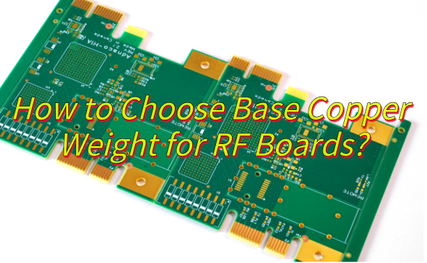
How to choose base copper weight for RF board? Let’s explore base copper weight options, selection guide, cost optimize solution, recommended supplier for RF board.
Are you troubled with these problems?
- Severe signal attenuation?
- Uncontrolled temperature rise?
- Impedance fluctuations?
EBest Circuit (Best Technology) can provide solutions:
- Dynamic copper thickness algorithm reduces skin loss by 40%.
- Gradient copper structure reduces hotspot temperature by over 15°C.
- Intelligent impedance compensation with a ±0.5μm tolerance ensures 5G+ accuracy.
Welcome to contact us if you have any inquiry for RF boards: sales@bestpcbs.com.
What Is Base Copper Weight?
Base Copper Weight refers to the thickness of the initial copper foil on the PCB substrate (usually measured in ounces per square foot or microns). It directly affects the circuit’s current carrying capacity, signal transmission stability, and thermal management performance. It is a core parameter in PCB design that balances conductivity, heat dissipation requirements, and manufacturing feasibility.
Why Base Copper Weight is Important for RF Boards?
Reasons why base copper weight is important for RF boards:
- Impedance Control: Base copper weight directly determines impedance accuracy (e.g., 50Ω for RF), minimizing signal reflection/loss.
- Thermal Management: Thicker copper (≥2oz) enhances heat dissipation, reducing temperature rise by 20-30% in high-power RF modules.
- Signal Loss Reduction: Low-profile copper (surface roughness <2μm) cuts high-frequency signal attenuation by ~30%.
- Mechanical Reliability: Thick copper (≥1.5oz) improves resistance to vibration/bending, preventing circuit failures.
- Process Compatibility: Base copper weight affects etching/lamination precision; thin copper suits fine lines but requires careful parameter tuning.
Common Base Copper Weight Options for RF Boards
1. 0.5 oz Copper(Thickness ≈17.5μm)
- Application: Core for millimeter-wave high-frequency (>30GHz) and precision impedance lines.
- RF strength: lowest skin effect loss, optimal signal integrity.
- Limitation: weak current capacity (<5A/mm²).
2. 1.0 oz Copper( Thickness ≈35μm)
- Application: Standard for mainstream RF circuits (5G/WiFi6).
- RF strength: balanced impedance control & current carrying (10-15A/mm²).
- Limitation: slightly higher high-frequency loss than 0.5oz.
3. 2.0 oz Copper (Thickness ≈70μm)
- Application: Designed for high-power RF modules (base stations/radars).
- RF strength: 3x current capacity, 40% higher thermal efficiency.
- Limitation: significant loss increase at >10GHz.
3. 3.0 oz+ Copper(Thickness ≥105μm)
- Application: Used for high-current power supplies (e.g., phased array antennas).
- RF strength: supports extreme current (>30A/mm²).
- Limitation: requires etching compensation, >50% cost increase.
4. Hybrid Copper Solutions(Customizable thickness)
- Application: For multilayer boards (signal + power layers).
- RF strength: surface layer 0.5oz minimizes loss, inner layer 2oz enhances current.
- Limitation: high process complexity, increased lamination cost.
How to Choose the Base Copper Weight for RF Boards?
1. Define High-Frequency Requirements & Loss Budget
- Evaluate RF circuit loss budget (dB): Based on signal frequency, transmission distance, and acceptable loss, determine the maximum per-unit-length loss.
- Copper thickness impact on conductor loss: At high frequencies, the skin effect concentrates current near the surface; thicker copper reduces conductive loss. RF signal layers typically use 0.5-2 oz base copper.
2. Prioritize Impedance Control
- Strictly match impedance targets (e.g., 50Ω transmission lines): Base copper weight is critical for impedance calculations and must align with dielectric thickness, trace width, and spacing.
- Example: 50Ω Grounded Coplanar Waveguide (GCPW)
- Base copper: 0.5 oz (≈17.5 μm)
- Trace width: 6 mil, ground gap: 10 mil
- Dielectric thickness: 3.8 mil (Dk=4.1)
3. Consider Copper Foil Roughness for High-Frequency Loss
- Surface roughness impact: Rough copper significantly increases loss at microwave frequencies.
- Recommended low-roughness foils: VLP (Very Low Profile): Roughness (Rq) ≈0.68 μm; RTF (Reverse Treat Foil): Roughness ≈2.6 μm.
4. Layer-Specific Copper Weight Selection
Signal layers:
- Use 0.5 oz or 1 oz to balance loss and etching precision. Thicker copper (≥2 oz) complicates etching and limits minimum trace/space.
Power/ground planes
- Prioritize 2 oz to 6+ oz to minimize resistance and thermal stress.
Internal layers:
- Signal layers: 0.5 oz for trace width <0.127 mm to enhance etching accuracy.
- Plane layers: 1 oz for cost efficiency; 2 oz requires ≥10 mil spacing and adds ~20% cost.
5. Account for Manufacturing Constraints
Minimum trace/space rules:
- 1 oz boards: Outer layers ≥5 mil (2-layer) or ≥3.5 mil (4/6-layer).
- 2 oz boards: All layers ≥8 mil.
Lamination structure:
- 4-layer PCBs: Internal copper options—0.5 oz, 1 oz, or 2 oz (≥1.6 mm thickness required for 2 oz).
- Plating impact: Final copper thickness (e.g., after ENIG) must include design margins.
6. Cost-Material Optimization
- Standard weights (0.5/1/2 oz) are cost-effective; custom thicknesses require special processes and increase costs.
- High-frequency laminates: e.g., Rogers RO4003C often pairs with 0.5 oz (≈17 μm) base copper for stable dielectric properties.
- Cost-sensitive designs: Use FR-4 with 1 oz copper; for >5 GHz, combine optimized copper with RF laminates.
How Does Base Copper Weight Impact RF Board Production Cost?
1. Material Cost & Copper Thickness
- Impact: Each 1 oz (≈35μm) copper increase raises raw material cost by 30-50%; >3 oz requires special rolling, costing exponentially more.
- Solution: Prioritize standard weights (0.5/1/2 oz) for scalability; use “localized thick copper” (e.g., 2 oz only for power planes) to avoid full-board waste.
- Example: 5G base stations reduce cost 15-20% by pairing 1 oz signal layers with 2 oz power planes.
2. Etching Complexity Control
- Impact: Thick copper (≥2 oz) causes undercut, extending etching time 20-40% and increasing depreciation costs.
- Solution: Adopt Semi-Additive Process (SAP) or optimized etchants (e.g., acidic cupric chloride); design with 10% width compensation for 2 oz traces to minimize rework.
3. Trace/Space Design Optimization
- Impact: 2 oz copper requires ≥8 mil trace/space, limiting density and potentially increasing layer count or expensive processes.
- Solution: Use 0.5 oz for signal layers (supports 3.5-5 mil) with HDI microvias; balance with 1 oz for non-critical layers.
4. Lamination & Drilling Efficiency
- Impact: Thick copper needs higher temp/pressure (200°C/400 psi) and longer press cycles (120 min); drilling wear increases costs 10-25%.
- Solution: Optimize drilling parameters (such as coated drills) and pre-stack structures to reduce press cycles; use high-temp rapid lamination.
5. Surface Finish & Plating Cost Control
- Impact: Thick copper extends plating time, increasing chemical use (5-15% cost rise).
- Solution: Shorten plating with efficient additives; replace ENIG with OSP in non-HF areas; optimize plating line layout to reduce copper waste.
6. Yield Improvement & Defect Prevention
- Impact: Thick copper reduces yield by 5-10%; thin copper risks wrinkling/breakage.
- Solution: Deploy AOI for real-time etching monitoring; reinforce thin copper with support layers; optimize stack-up to reduce interlayer stress, targeting >95% yield.
7. Supply Chain & Economies of Scale
- Impact: Custom weights require premium pricing and longer lead times, increasing inventory/logistics costs.
- Solution: Partner with fabricators for pooled standard weight inventory; use panelization for custom orders to share fixed costs; explore cost-effective alternatives like Cu-Al composite foil.
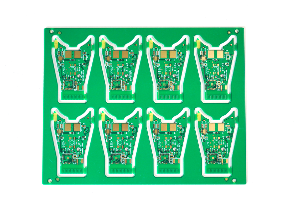
Why Choose EBest Circuit (Best Technology) as RF Board Manufacturer?
19-Year PCB Manufacturing Expertise & Global Certifications:
- ISO 9001, ISO 13485, UL and RoHS compliance guarantee product safety and regulatory adherence.
24 Hours Rapid Prototyping
- Quick-turn prototypes (24-72 hours) with DFM feedback to optimize copper weight, stack-up, and impedance before volume production.
Multi-Thickness Copper Base Selection
- Offer flexible base copper weights (0.5 oz to 6+ oz) to match diverse RF requirements, from ultra-low-loss 0.2 oz for millimeter-wave designs to robust 6 oz for high-power applications.
Advanced Impedance Control Expertise
- Precision engineering for 50Ω/75Ω transmission lines with sub-1% impedance tolerance, supported by co-simulation of copper weight, trace geometry, and dielectric parameters.
Low-Loss Material Integration
- Compatibility with high-frequency laminates (e.g., Rogers RO4000/RT/duroid, Panasonic Megtron 6) and optimized copper foil roughness (VLP/RTF) to minimize insertion loss.
High-Density Interconnect (HDI) Capability
- Enable ≥20μm line/space resolution via SAP/mSAP processes, supporting complex RF module integration with minimal signal degradation.
Thermal Management Solutions
- Design-integrated thick copper planes (≥2 oz) with thermal vias and heat sinks to enhance heat dissipation in GaN/HEMT power amplifiers.
Cost-Performance Optimization
- Balanced material selection (e.g., FR-4 for cost-sensitive layers, RF laminates for critical signal paths) to minimize overall BOM cost while meeting performance targets.
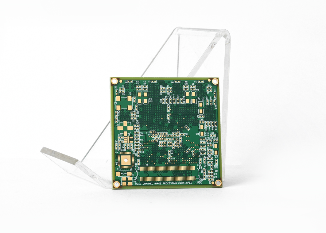
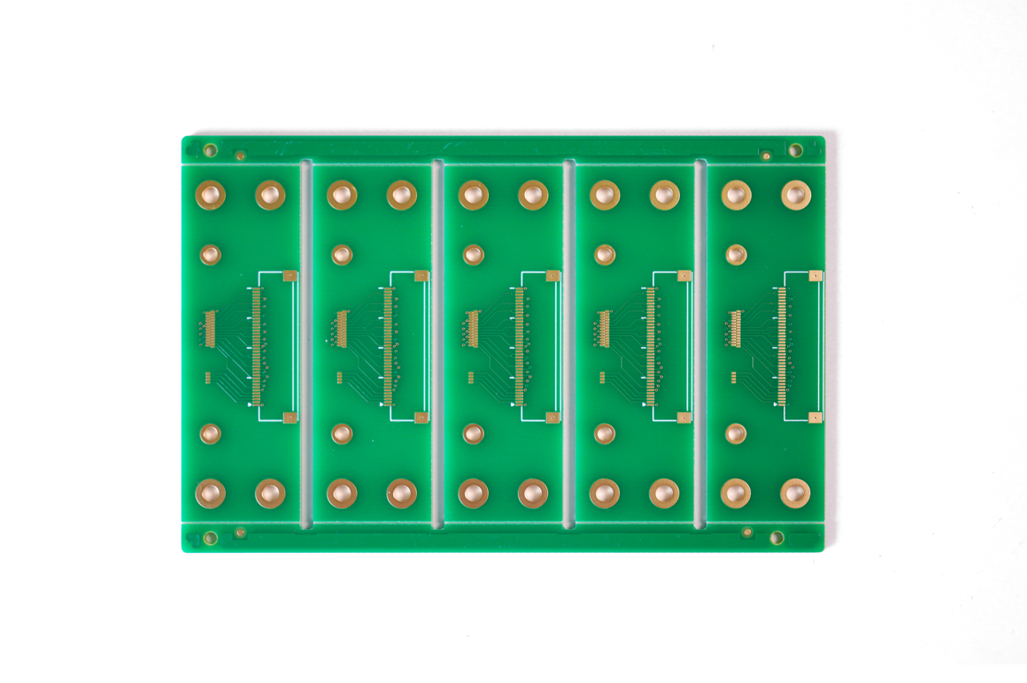
Our RF Board Capabilities
| Base material: | Rogers/Telfon |
| Board Thickness: | 0.5mm~3.0mm(0.02″~0.12″) |
| Copper thickness: | 0.5 OZ, 1.0 OZ, 2.0 OZ, 3.0 OZ |
| Outline: | Routing, punching, V-Cut |
| Soldermask: | White/Black/Blue/Green/Red Oil |
| Legend/Silkscreen Color: | Black/White |
| Surface finishing: | Immersion Gold, HASL, OSP |
| Max Panel size: | 600*500mm(23.62″*19.68″) |
| Packing: | Vacuum/Plastic bag |
| Samples L/T: | 7~9 Days |
| MP L/T: | 8~10 Days |
How to Get a Quote for RF Board Project?
List of items to submit for quotation:
1. Technical Specifications
- Layer count (e.g., 4-layer rigid-flex).
- Base material (e.g., Rogers 4350B, FR4).
- Copper weight (e.g., 1oz outer/2oz inner).
- Impedance control requirements (±5% tolerance).
- Surface finish (e.g., ENIG, Immersion Silver).
2. Design Files
- Gerber files (RS-274X format).
- Drill files (Excellon format).
- IPC-356 netlist (for testing).
3. Special RF Requirements
- Frequency range (e.g., 5-40GHz).
- Insertion loss limits (e.g., <0.5dB/inch @10GHz).
- RF-specific stackup (e.g., hybrid PTFE/FR4).
4. Production Details
- Quantity (prototype/bulk order).
- Delivery timeline (e.g., 4-week lead time).
- Testing standards (e.g., IPC-6012 Class 3).
5. Additional Notes
- Special tolerances (e.g., ±2mil line width).
- Certifications (e.g., UL, ITAR).
- Packaging requirements (vacuum-sealed).
Welcome to contact us if you have any request for RF boards: sales@bestpcbs.com.
Tags: base copper weight