

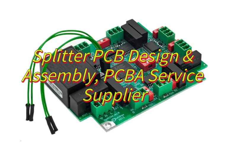
What is splitter PCB? Let’s explore its function, types, applications, technical parameter, design guide, assembly processes through this blog.
Customer Pain Points and Difficulties:
- Severe signal attenuation and short transmission distance? (Splitter PCB uses high-precision impedance matching to ensure lossless signal distribution and extend transmission distance.)
- Multi-path signal interference and poor stability? (Splitter PCB’s optimized isolation design effectively suppresses EMI/EMC and ensures signal purity.)
- Complex assembly process and low yield? (Splitter PCB’s standardized production process and automated SMT placement improve consistency.)
EBest Circuit (Best Technology) can provide services and solutions:
Customized Design Support: Provide impedance simulation and stack up optimization to ensure Splitter PCB meets your signal distribution needs.
Efficient Production and Delivery: 7-day proofing and 15-day mass production, quickly responding to your project schedule.
Full-Process Quality Assurance
ISO 9001 control throughout the entire process, from PCB manufacturing to assembly and testing, ensures reliability.
Let EBest Circuit (Best Technology) be your splitter PCB expert and solve your signal distribution challenges! Contact us now if you have any request for splitter PCB design and assembly: sales@bestpcbs.com.
What is Splitter PCB?
A splitter PCB is a printed circuit board (PCB) specifically designed for signal or power distribution. It distributes input signals/currents to multiple output ports in equal or unequal proportions, enabling system signal synchronization or power isolation.
What is the Purpose of Splitter PCB?
- RF Signal Distribution: Used in communications equipment (such as base stations and routers), it splits RF signals into multiple channels.
- Mixed Signal Isolation: Isolates noise interference from analog and digital circuits.
- Power Management: Distributes different voltage rails in multi-voltage systems (such as automotive BMS).
- High-Speed Interface Optimization: Improves the transmission stability of high-speed signals such as PCIe/USB4.
- Test Support: Facilitates device debugging and performance monitoring.
- Flexible Electronics Integration: Adapts to the compact space requirements of wearable devices and foldable displays.
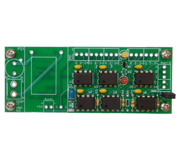
What Are Types of Splitter PCB?
- POE Splitter PCB: Separates Power over Ethernet (PoE) into data and power, adapting to non-PoE devices.
- Audio Splitter PCB: Distributes audio signals to multiple output channels (such as 3.5mm/RCA jacks), supporting parallel connection of speakers or headphones.
- Fan Splitter PCB: Connects multiple fans (12/24V) in parallel, simplifying wiring for cooling systems (such as 3D printers or chassis fans).
- HDMI Splitter PCB: Duplicates a single HDMI signal to multiple displays, supporting 4K/8K video transmission (such as conference presentations or advertising screens).
- USB Splitter PCB: Expands a single USB port into multiple ports, supporting peripheral connection or charging (such as keyboards, mice, and mobile phones).
What Are Applications of PCB Splitter?
- Communications and RF Systems – Signal distribution (such as 1-to-2 splitters), frequency band division (broadband equal power division), and RF test equipment (connecting signal sources and measuring instruments).
- Audio Equipment – Speaker crossover (high/mid/low frequency band distribution), electronic crossovers (weak signal division before amplifiers).
- Automotive Electronics – Power control (motor controllers, battery management systems), intelligent driving (millimeter-wave radar high-frequency PCBs), new energy battery data acquisition cables (FPC flexible monitoring).
- Consumer Electronics – Smartphones/tablets (HDI boards, flexible PCBs), wearable devices (lightweight and heat-resistant designs).
- Industrial and Aerospace – Extreme environments (high temperature/high pressure/strong electromagnetic interference), high-precision control (multilayer boards, ceramic substrates).
- Data Centers and Cloud Computing – High-speed signal transmission (servers, data center multilayer boards), low-latency data processing.
- Smart Home and IoT: Wireless device integration (sensors, communication modules), low-power flexible PCB design.
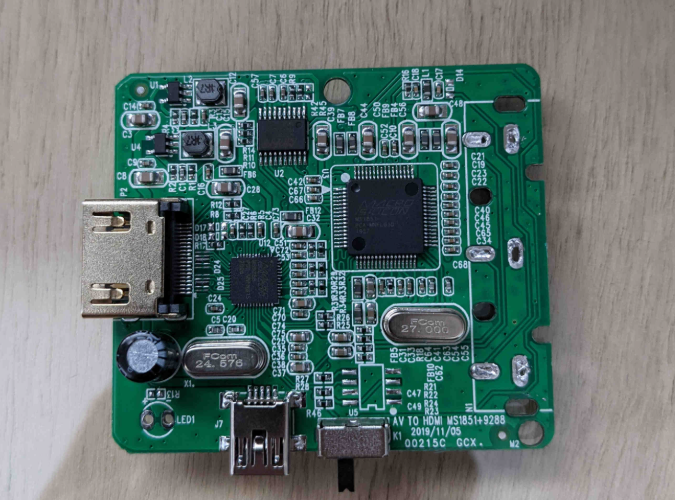
HDMI Splitter PCB Design Technical Parameter
| Parameter Category | Technical Specifications |
| Input/Output Interface | 1×HDMI input, 2×/4×/8×HDMI outputs (configurable) |
| HDMI Version Support | HDMI 2.0b/2.1 (supports 4K@60Hz, HDR, HDCP 2.2/2.3) |
| Resolution Support | Maximum 4K@60Hz (4:4:4), compatible with 1080P/720P and below |
| Signal Bandwidth | 18Gbps (HDMI 2.0) / 48Gbps (HDMI 2.1) |
| Operating Voltage | DC 5V (typical) |
| Power Consumption | ≤5W (static), ≤10W (dynamic) |
| PCB Layers | 4-6 layer board (impedance-controlled layers) |
| PCB Material | FR-4 (Tg≥170℃), optional high-frequency material (e.g., Rogers 4350B) |
| Differential Impedance | 100Ω±10% (HDMI differential signal lines) |
| Signal Integrity | Insertion loss ≤-3dB@6GHz, return loss ≤-10dB@6GHz |
| EDID Support | Dynamic/Static EDID storage (EEPROM capacity ≥256Byte) |
| HDCP Support | HDCP 1.4/2.2/2.3 compliant |
| Connector Type | HDMI Type A female socket (gold-plated contacts, thickness ≥15μm) |
| ESD Protection | Human Body Model ±8kV, Machine Model ±200V (IEC 61000-4-2) |
| Operating Temperature | 0℃~70℃ (commercial grade), optional -40℃~85℃ (industrial grade) |
| Certification Standards | CE, FCC, RoHS, HDMI Adopter Certification |
How to Design a HDMI Splitter PCB?
HDMI splitter PCB design guide:
1. Basic Layout and Stackup Design
Shortening the signal path:
- Minimize the distance between the HDMI connector and the processing chip (such as the TMDS341A) to reduce signal attenuation and EMI.
Stackup Structure:
- Use at least a 4-layer PCB (6 layers recommended), including a complete power and ground layer.
- High-speed signal layers should be placed adjacent to the ground layer to enhance magnetic field coupling and suppress EMI.
2. Differential Signal Impedance Control (100Ω)
Trace Rules:
- A 1:1 differential pair width/space ratio is recommended, with intra-pair error ≤ 5 mil and inter-pair error ≤ 10 mil.
- Trace spacing (s) must meet the following requirements:
s < h(dielectric thickness),s < W(line width), andd > 2s(distance from other traces). - Use a 2D field solver to accurately calculate impedance, avoiding reliance on empirical values.
Via Design:
- Use small vias (8 mil/16 mil recommended) to reduce capacitance effects and impedance drop.
- Avoid switching high-speed signals across different layers; otherwise, additional return vias will be required.
3. Power Supply and Decoupling Capacitor Design
- Power Inlet: Place a 10μF tantalum capacitor for voltage regulation.
- Chip Power Supply: Place a 0.1μF or 0.01μF ceramic capacitor next to each high-speed chip, and connect the capacitor pins with double vias to reduce inductance.
- Decoupling Capacitors: Configure at least one 4.7μF capacitor and five 0.1μF capacitors, connecting them directly to the power plane (minimizing the path).
- Power Plane: Avoid signal lines crossing split planes to ensure a continuous return path.
4. EDID Management Strategy
- EDID Compose Mode: Automatically analyzes the resolutions of all displays and selects the lowest compatible value (e.g., 1080P) to ensure compatibility.
- Fixed Mode: Forces the output to a specific resolution (e.g., 4K@60Hz) to accommodate high-end devices.
- Priority Setting: Supports port priority (for example, when Output 1 is disconnected, Output 2 defaults to 1080P)
5. Design for Manufacturability (DFM)
Trace Equal Length:
- Length deviation within a differential pair should be ≤ 5 mil to prevent EMI caused by phase shift.
- Use curved or serpentine traces to correct for length differences.
Pad and Spacing:
- HDMI pads should be minimized to prevent impedance mismatch.
- The copper pad to board margin distance should be ≥ 75 mil to meet production process requirements.
6. Expandable Functionality and Compatibility
Output Port Planning:
- Select the number of ports based on requirements (e.g., 1×2/1×4), and reserve one or two spare ports for upgrades.
Supported Protocols:
- Ensure support for HDCP 1.4+/HDMI 2.0, 4K@60Hz, and 3D formats.
- Integrate CEC commands (e.g., one-button standby and remote control passthrough) to enhance the user experience.
External Power Supply:
- Multiple ports (≥4 outputs) require a separate 12V/5A power supply to avoid power shortages.
7. Design Considerations
- Avoid Cross-Splits: A complete reference plane is required beneath the differential lines, otherwise impedance jumps and noise will occur.
- Capacitor Selection: Use low-ESL ceramic capacitors for high-frequency ranges (>100MHz) and tantalum capacitors for voltage stabilization in low-frequency ranges.
- Connector Quality: Use connectors that meet HDMI impedance standards to avoid signal reflections.
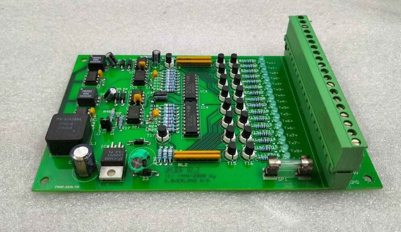
How to Assemble a Splitter PCB?
Below are splitter PCB assembly processes:
1. Prepare Materials & Tools
- Gather Splitter PCB (pre-etched), component kit (resistors, capacitors, transmission lines), solder wire, flux, soldering iron, tweezers, multimeter.
- Inspect PCB for cleanliness and shorts; verify components match BOM (e.g., resistor values).
2. Component Placement
Align components with PCB silkscreen:
- Insert resistors/capacitors into pads; press gently.
- Embed transmission lines (e.g., quarter-wavelength microstrip) into slots, ensuring contact with pads.
- High-frequency parts (e.g., Wilkinson resistors) must follow polarity marks.
3. Soldering
- Set iron to 280–320°C (use lower temp for PTFE to avoid warping).
- Steps:
a. Apply flux to pad/lead.
b. Feed solder until melted; remove iron for smooth joints.
c. Use “drag soldering” for SMD parts. - Focus: Transmission line joints and isolation resistors (avoid cold joints/bridges).
4. Quality Inspection
- Visual check: Conical, shiny solder joints with no cracks.
- Electrical test: Measure resistance (e.g., isolation resistors) with multimeter (≤5% deviation).
- Continuity test: Short input to one output; others should show no connection.
5. Functional Verification
- Connect signal generator and spectrum analyzer:
a. Input signal to PCB; measure output power (e.g., 1-to-2 divider: ≤0.5dB difference).
b. Test port isolation (e.g., ≤-20dB). - Debug: Re-solder components if power imbalance or poor isolation persists.
6. Cleaning & Protection
- Wipe flux residue with alcohol to prevent corrosion.
- Apply conductive adhesive on edges for RF applications to reduce EMI.
- Package in anti-static bags with specs/test results labeled.
7. Notes:
- Use automated soldering for high-frequency PCBs (e.g., 77GHz automotive radar) to avoid parameter shifts.
- Prioritize network analyzers for testing; multimeters suit low-frequency checks only.
Why Choose EBest Circuit (Best Technology) as PCBA Service Supplier?
Reasons why choose us as splitter PCB assembly service supplier:
- 19 Years of Industry Experience: Proven expertise in RF/high-speed splitter PCB assembly for 5G, automotive, and IoT applications.
- Full Certification Compliance: ISO 9001, IATF 16949, ISO 13485 and RoHS, UL certified, and ensures global market compliance and reliability.
- Cost-Effective Solutions: Competitive pricing and optimized material sourcing help reduce your production costs by 15-30%.
- Free DFM & Design Support: Expert impedance matching (e.g., 50Ω RF traces) and signal integrity analysis ensure optimal splitter PCB performance.
- Reliable Quality Control: Strict process control with AOI/SPI/X-Ray inspection ensures 99.5% assembly yield and minimal defects.
- Fast Turnkey Assembly: 7-day prototype delivery and 15-day mass production for splitter PCB orders (100pcs–10Kpcs).
- Advanced SMT Capabilities: Supports 01005-size components and 0.3mm BGA assembly for high-density splitter PCB designs.
- Effective Signal Isolation: Dedicated EMI/EMC control measures prevent crosstalk in mixed-signal splitter boards.
- Flexible Scalability: Seamless transition from prototypes to large-scale production (1M+ units) with consistent quality.
- 24/7 Technical Support: Dedicated engineers provide real-time DFM feedback and troubleshooting support.
Welcome to contact us if you have any request for PCBA service: sales@bestpcbs.com.
Tags: PCB Splitter, Splitter PCB