

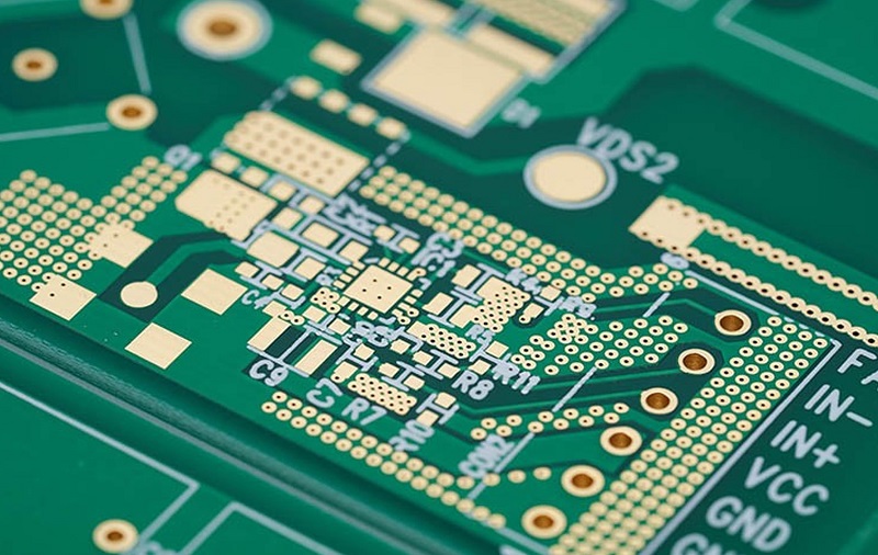
OSP surface finish is critical for HDI PCBs, especially when working with fine-pitch components and limited budget. It offers a flat, lead-free layer that keeps copper pads clean and solderable. That’s why many designers choose it for high-density layouts.
EBest Circuit (Best Technology) is a China PCB factory, offering a variety of true quality PCBs, such as HDI PCBs, high Tg PCBs, high speed PCBs, extra thin PCBs, etc. With certifications like ISO 9001, IATF 16949, ISO 13485, and AS9100D, we have a major competitive edge for strict quality control. If you require any PCB or PCB assembly, just contact us via call at +86-755-2909-1601 or via email at sales@bestpcbs.com. Our team is on call at any moment.
What is the OSP Surface Finish?
OSP stands for Organic Solderability Preservative. It’s a water-based organic layer applied over bare copper. This coating keeps copper from oxidizing before soldering. During assembly, the OSP dissolves, allowing solder to form a clean joint. It’s simple, safe, and perfect for mass production.
What Are the Different PCB Surface Finish Types?
There are several surface finish options in PCB manufacturing:
- OSP: Flat and affordable, ideal for HDI designs.
- HASL: Economical, but uneven for fine-pitch parts.
- ENIG: Smooth and reliable, but higher in cost.
- Immersion Silver: Great for signal integrity and RF use.
- ENEPIG: Durable and wire-bondable, suitable for high-reliability and gold wire applications.
Each has its purpose. OSP shines where planarity and cost-saving matter most.
What is the Relationship: OSP Surface Finish vs PCB?
The OSP surface finish vs PCB relationship lies in solderability and flatness. HDI PCBs have tight space and small pads. OSP helps keep those copper pads flat and clean. That’s key for 0.3mm BGAs or 01005 parts. Plus, it’s lead-free and RoHS compliant.
What is the Difference: HASL ENIG OSP Surface Finishing?
Here’s a comparison:
- HASL: Tin-based, uneven finish. Not good for HDI.
- ENIG: Gold over nickel. Smooth, long-lasting, but costly.
- OSP: Organic layer. Flat, low-cost, but sensitive to heat and moisture.
OSP is great when used right. For multi-reflow or harsh environments, ENIG may be better.
Here’s a quick look:
| Finish | Flatness | Durability | Cost | Best For |
| HASL | Low | Medium | Low | General-purpose |
| ENIG | High | High | High | Fine-pitch, critical zones |
| OSP | High | Medium-Low | Low | HDI, low-cycle reflow |
What is the OSP PCB Shelf Life?
Normally, OSP PCB shelf life is 3 to 6 months. After that, oxidation may start. To avoid this, EBest Circuit (Best Technology) uses vacuum-sealed bags with desiccants. Our storage process keeps boards clean and dry for up to 9 months. We also recommend using them within 90 days for the best results.
What is the OSP Surface Finish Process?
The OSP surface finish process involves several precise steps:
- Cleaning the copper pad: The surface must be free of oxidation, fingerprints, and oil. A thorough de-oiling step ensures uniform coating formation.
- Micro-etching: Copper is etched by 1.0–1.5 μm to create a slightly rough surface, which improves coating adhesion.
- Applying the organic coating: After etching, an organic layer is applied. The PCB is then rinsed with DI water, with pH strictly controlled between 4.0–7.0 to prevent damage to the coating.
- Drying and curing: The board is dried at 60–90 °C for about 30 seconds. The exact time and temperature depend on the OSP chemistry used.
- Solderability: The OSP layer thermally decomposes above 150 °C during soldering, exposing clean copper for reliable joint formation.
This detailed process results in a flat, solderable surface that supports high-density assembly without additional complexity or cost.
How Thick is OSP Surface Finish?
The typical thickness of OSP surface finish ranges from 0.2 to 0.5 μm, depending on the chemistry and application method. While 0.25 to 0.35 μm is a common range, it’s not the only standard. If the coating is too thin (below 0.2 μm), it may not offer adequate protection and can oxidize quickly. If it’s too thick (over 0.5 μm), it could hinder solder wetting. At EBest Circuit (Best Technology), we maintain strict control over the OSP thickness to ensure consistent solderability and long-term protection.
What Are the Applications for PCB Surface Finish OSP?
OSP is widely used in cost-sensitive and high-density designs, where flatness and affordability are key. Common applications include:
- Consumer electronics: Remote controls, home appliances, and other high-volume, cost-driven products often use OSP for its affordability.
- Wearables: Devices requiring lightweight, compact PCBs benefit from OSP, although it’s less ideal for assemblies requiring multiple reflows.
- Tablets and smartphones: OSP supports the flat pad requirements of HDI boards, commonly found in mobile devices.
- High-density boards: In PCBs with fine-pitch components or narrow spacing, OSP avoids bridging issues caused by thicker finishes like HASL.
- General SMT assemblies: Any design where smooth, flat pads are needed to ensure reliable solder joints at a lower cost.
However, OSP is not ideal for high-frequency signal boards (due to potential impedance variation) or assemblies requiring multiple reflow cycles, as the coating can degrade.
Why Choose OSP for HDI PCBs?
OSP is perfect for HDI. It’s flat, cheap, and lead-free. That’s a win for small components. But it does need care. At EBest Circuit (Best Technology), we’ve solved the main problems:
- Thermal issues? We use high-temp OSP that resists up to 3 reflows.
- Short shelf life? Our sealed packs extend life up to 9 months.
- Scratches or oxidation? Our handling uses trays and gloves only.
- Visual checks? We combine OSP for pads and ENIG for test points.
With the right practices, OSP works beautifully—even for 01005s. We guide clients on reflow profiles, alloy choices, and pad design to get the best result every time.
All in all, OSP surface finish is the right call for many HDI builds. It keeps costs down while giving solid results. But you need a partner who understands how to use it. That’s where EBest Circuit (Best Technology) leads. Our OSP+ solutions allow for better thermal handling and longer shelf life. Plus, with careful design and packaging, you avoid common issues before they happen.
For designs with ≤3 reflows, OSP is a top choice. For mixed assemblies, hybrid OSP/ENIG works even better. A warm welcome to make a call to us at +86-755-2909-1601 to discuss more of your project details or email the Gerber files and your special requirements to us at sales@bestpcbs.com.
Tags: OSP Surface Finish