

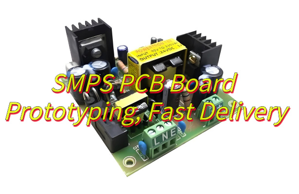
Seeking for SMPS PCB Board solutions? This guide explores its definition, functions, applications, design strategies, and fast-delivery advantages.
EBest Circuit (Best Technology) specializes in high-quality SMPS PCB board prototyping and assembly services with industry-leading 24-hour quick-turn delivery. Our accelerated production process ensures fast turnaround without compromising quality, supported by:
- Free professional DFM analysis to optimize designs for manufacturability
- Advanced fabrication capabilities (up to 20-layer boards, 6oz copper)
- Full IPC-A-600 compliant quality control with flying probe testing
- Mixed-technology assembly (SMT+THT) for complex power electronics
With 18+ years of SMPS manufacturing experience, we maintain <1% defect rate through rigorous process controls. Our engineering team provides actionable DFM feedback to reduce prototyping iterations. Clients benefit from our one-stop solution combining rapid delivery (50% faster than industry average), cost efficiency, and reliable performance – validated by 95%+ repeat order rate from global power supply manufacturers. Welcome to contact us: sales@bestpcbs.com.
What Is SMPS PCB Board?
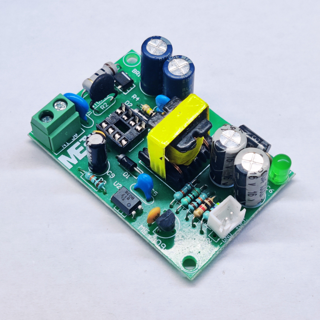
A SMPS (Switched Mode Power Supply) PCB board serves as the core component in power conversion systems, efficiently transforming and regulating electrical energy for various applications. These boards incorporate essential elements such as transformers, MOSFETs, diodes, and control ICs arranged on a compact layout to enable high frequency switching and minimize power loss. During prototyping, engineers focus on optimizing trace routing, thermal dissipation, and EMI suppression to enhance performance and reliability under different operating conditions.
For rapid prototyping and fast delivery, manufacturers employ efficient design validation techniques and accelerated PCB fabrication processes. Automated testing and iterative refinements help ensure the board meets specifications before full scale production. Material choices, including heat resistant laminates, contribute to durability in demanding environments. Whether used in industrial machinery or consumer electronics, SMPS PCB boards play a vital role in delivering stable, energy efficient power solutions.
What Is the Function of the SMPS Board?
Here are functions of an SMPS board:
- Efficient Power Conversion: Switches power at high frequencies to minimize energy loss, reducing electricity costs and heat generation compared to traditional power supplies.
- Voltage Transformation: Converts higher input voltages (AC or DC) to precisely regulated lower DC voltages needed by electronic devices, ensuring proper operation.
- Noise Suppression: Incorporates filters to eliminate electrical interference, preventing disruptions to nearby devices and maintaining signal integrity.
- Thermal Management: Uses heatsinks and thermal design to dissipate heat effectively, prolonging component life and maintaining reliable performance.
- Overload Protection: Automatically shuts down during power surges or short circuits, safeguarding both the power supply and connected equipment from damage.
- Compact Design: High-frequency operation allows smaller components, enabling lightweight and space-saving solutions for modern electronics.
- Wide Input Range: Adapts to varying input voltages automatically, making devices compatible with different power standards worldwide.
- Stable Output Regulation: Maintains constant voltage output despite fluctuations in input power or load changes, ensuring consistent device performance.
What Are Applications of SMPS PCB Board?
Applications of SMPS PCB board:
- Consumer Electronics Power Supplies – Provides compact, efficient power conversion for devices like televisions, gaming consoles, and audio systems, enabling slimmer product designs while reducing energy consumption.
- Computer and Server Power Systems – Delivers stable multi-voltage outputs for motherboards, storage devices, and processors, ensuring reliable operation while minimizing heat generation in confined spaces.
- Industrial Equipment Control – Supplies regulated power to automation systems, PLCs, and motor drives with robust protection against voltage fluctuations common in manufacturing environments.
- Telecommunications Infrastructure – Maintains uninterrupted power for network switches, routers, and base stations, featuring high efficiency to reduce operational costs in always-on applications.
- Medical Device Power Management – Provides ultra-clean power with strict noise suppression for sensitive diagnostic equipment, meeting rigorous safety standards for patient-connected devices.
- LED Lighting Drivers – Enables precise current regulation for commercial and residential lighting systems, improving energy efficiency while extending LED lifespan.
- Renewable Energy Systems – Facilitates power conversion in solar inverters and battery storage systems, maximizing energy harvest while adapting to variable input conditions.
- Transportation Electronics – Powers onboard systems in electric vehicles, trains, and aircraft with vibration-resistant designs that withstand harsh mobile environments.
Design Consideration of SMPS PCB Board
Optimized Design Considerations for SMPS PCB Boards
Circuit Partitioning and Signal Integrity
- Segregate high-voltage and low-voltage sections: Isolate switching nodes (e.g., MOSFETs, transformers) from sensitive analog/digital circuits (e.g., feedback resistors, control ICs) using guard rings or ground gaps. This reduces crosstalk and improves signal clarity.
- Optimize grounding strategy: Designate separate ground planes for power stages and control logic, connecting them at a single point to prevent ground loops. For example, route PWM controller grounds away from high-current paths.
Component Placement and Routing
- Prioritize high-current paths: Place inductors, output capacitors, and connectors close to load terminals to minimize trace resistance. For instance, align output capacitors parallel to inductors to reduce loop inductance.
- Shorten switching node traces: Route high-frequency loops (e.g., MOSFET drain to transformer) with minimal length and width to mitigate electromagnetic interference (EMI). Use polygon pours for critical nodes to lower impedance.
Thermal Management
- Maximize heat dissipation: Add thermal vias under power devices (e.g., MOSFETs, rectifiers) to conduct heat to inner layers or external heatsinks. For example, use a 10–20 via array under a TO-220 package.
- Use copper zones strategically: Design solid copper pours for high-power traces (e.g., 2 oz. copper for VIN/VOUT rails) and avoid thermal reliefs to enhance thermal conductivity.
EMI/EMC Compliance
- Filter input/output noise: Integrate EMI filters (e.g., ferrite beads, X/Y capacitors) at AC/DC ports to suppress conducted emissions. For example, place a common-mode choke before the bridge rectifier.
- Control impedance: Maintain 50Ω differential impedance for high-speed signals (e.g., PWM drivers) using PCB stack-up planning and controlled dielectric spacing.
Safety and Creepage Distances
- Adhere to safety standards: Ensure ≥6mm creepage between primary and secondary circuits for 250VAC isolation. Use slotted PCB cutouts or insulating barriers if space is constrained.
- Reinforce high-voltage isolation: Apply solder mask dams or conformal coatings to protect against dust accumulation in creepage areas.
Design for Manufacturing (DFM)
- Standardize footprints: Use preferred component libraries (e.g., 0805 resistors, SOIC-8 ICs) to streamline assembly and reduce procurement delays.
- Avoid tight tolerances: Specify ≥0.2mm annular rings and ≥0.15mm solder mask slivers to accommodate manufacturing variations.
Why Choose SMPS PCB Board Prototyping?
Reasons why choose SMPS PCB board prototyping:
Accelerated Time-to-Market
- Rapid prototyping shortens development cycles by enabling iterative testing of power conversion topologies (e.g., flyback, forward, or LLC resonant converters).
- Modular PCB layouts and off-the-shelf components allow quick adjustments to voltage rails, efficiency targets, or thermal performance without full redesigns.
Cost-Efficient Design Validation
- Prototyping identifies flaws (e.g., EMI hotspots, thermal bottlenecks) early, preventing costly reworks during mass production.
- Low-cost materials or hybrid PCB technologies (e.g., combining FR-4 with metal-core substrates) can be used for initial testing before finalizing high-volume specifications.
Risk Mitigation Through Testing
- Early-stage validation of critical parameters—such as load regulation, transient response, and efficiency under varying input voltages—reduces failure risks in end-products.
- Automated test equipment (ATE) integration during prototyping ensures compliance with safety/EMC standards, avoiding post-certification delays.
Customization for Diverse Applications
- Prototyping supports tailored solutions for industries like automotive (high-temperature resilience), medical (low leakage current), or renewable energy (wide input range).
- Adjustable features (e.g., programmable output voltages, digital control interfaces) can be tested before committing to fixed designs.
Supply Chain and Manufacturing Readiness
- Collaborating with PCB manufacturers during prototyping ensures alignment with DFM (Design for Manufacturing) guidelines, such as panelization, solder paste optimization, and component availability.
- Early engagement with assembly houses helps identify potential issues (e.g., stencil design, pick-and-place feasibility) for smoother production ramps.
How to Optimize SMPS PCB Prototype Design to Reduce Costs?
Simplify Circuit Topology
- Use common topologies: Select flyback or buck converters for non-critical applications to minimize components and design complexity.
- Avoid over-engineering: Align performance (e.g., efficiency, transient response) with actual needs instead of adding unnecessary features.
Leverage Standard Components
- Choose off-the-shelf parts: Prioritize generic MOSFETs, diodes, and capacitors over specialized or high-precision alternatives.
- Use wide-range components: Select parts with broad operating margins (e.g., 40–100V input for a 48V system) to reduce inventory.
Optimize PCB Layer Count
- Design with 2–4 layers: Strategically place ground/power planes and use thicker copper (e.g., 2 oz.) for high-current traces to avoid extra layers.
- Combine traces: Route signal and low-speed power lines on the same layer to simplify layout.
Adopt Modular Design
- Create reusable modules: Build EMI filter blocks or feedback loops that work across multiple prototypes.
- Use connectors for optional features: Add jumpers or connectors for non-essential functions (e.g., digital interfaces) to avoid redundant PCB spins.
Prioritize DFM Guidelines
- Collaborate with manufacturers: Align designs with PCB maker capabilities (e.g., panelization, solder stencils) to cut assembly costs.
- Relax tolerances: Avoid tight specs for holes, solder mask, or spacing unless critical for performance.
Outsource Non-Core Tasks
- Partner with specialists: Delegate tasks like magnetic component winding or thermal testing to firms with economies of scale.
Iterate With Low-Cost Materials
- Start with FR-4: Use standard FR-4 for initial prototypes instead of premium laminates (e.g., Rogers 4350B).
- Test thermal performance: Try solder mask or coatings before upgrading to metal-core PCBs.
How to Verify Performance Indicators in the Early SMPS Prototyping Stage?
How to Verify Performance Indicators in the Early SMPS Prototyping Stage
Leverage Simulation Tools
- Use SPICE-based software to model circuit behavior, such as switching losses and loop stability, before building physical prototypes.
- Simulate extreme conditions like input voltage fluctuations or overload scenarios to uncover weaknesses in control logic or component ratings.
Test Main Parameters Under Real-World Conditions
- Measure efficiency across the entire operating range using a programmable DC load and precision multimeter.
- Validate load transient response with a step load generator to ensure output voltage stability during sudden current changes.
Conduct Thermal Stress Testing
- Operate the prototype continuously at maximum rated load while monitoring component temperatures with thermal cameras or IR guns.
- Verify thermal performance against component derating curves to prevent premature failure or aging.
Perform EMI Pre-Compliance Checks
- Use a spectrum analyzer and near-field probe to detect radiated emissions from switching nodes or layout hotspots.
- Test conducted emissions by injecting noise into power lines and measuring filtering effectiveness with a LISN.
Automate Repetitive Tests
- Develop scripts for oscilloscopes or ATE systems to log data like ripple voltage or switching frequency over extended periods.
- Automate safety tests, such as overvoltage/overcurrent shutdown triggers, to reduce manual effort and errors.
Validate Component Tolerances
- Test worst-case scenarios by combining component tolerances in simulations or hardware adjustments.
- Use adjustable components like trimmer potentiometers to evaluate stability margins in feedback loops.
Iterate With Rapid-Prototyping Techniques
- Build breadboards or perfboard prototypes to quickly validate critical subcircuits like snubbers or gate drivers.
- Use PCB milling or low-cost fabrication services for fast turnaround of revised layouts.
Document and Analyze Failures
- Record test conditions, waveforms, and failure modes in a centralized database to track design improvements.
- Perform root-cause analysis for issues like instability or excessive ripple using structured methodologies.
How Can Prototyping Accelerate the Delivery Timeline for SMPS PCB Boards?
How Can Prototyping Accelerate the Delivery Timeline for SMPS PCB Boards?
Enable Rapid Iteration
- Use 3D printing or CNC machining to create mechanical mockups quickly, testing form factors before finalizing PCB layouts.
- Deploy in-house PCB milling machines to produce prototypes within hours, bypassing external fabrication delays.
Adopt Modular Design Principles
- Break the design into reusable modules (e.g., power stage, control board) for independent development and testing.
- Standardize interfaces (e.g., connectors, protocols) to enable parallel work on subsystems.
Leverage Simulation for Early Validation
- Use electromagnetic field (EMF) solvers to optimize high-frequency trace routing and mitigate EMI risks pre-hardware.
- Simulate thermal performance with CFD tools to identify hotspots and adjust component placement proactively.
Implement Concurrent Engineering
- Begin PCB layout while sourcing components, using predictive analytics to manage lead times for critical parts.
- Collaborate with firmware developers to integrate control algorithms during prototyping, avoiding sequential delays.
Use Off-the-Shelf Evaluation Boards
- Adapt vendor-provided reference designs for core functionality (e.g., PWM controllers) to reduce low-level debugging.
- Customize only unique features (e.g., auxiliary rails, protections) after validating baseline performance.
Automate Testing and Documentation
- Develop scripts for ATE systems to validate efficiency, ripple, and transient response in minutes.
- Generate compliance reports (e.g., EMI, safety) automatically using test data pipelines, cutting documentation time by 50%.
Prioritize Design for Manufacturing (DFM) Early
- Share PCB designs with contract manufacturers during prototyping to address DFM issues (e.g., panelization, solderability) upfront.
- Use CM-provided design rules to avoid costly re-spins later in production.
Conclusion
SMPS PCB prototyping enables efficient power supply development through optimized design, cost control, and early performance validation. By addressing key considerations and leveraging rapid prototyping, you can accelerate time-to-market while ensuring reliability. For competitive pricing and expert support, contact EBest Circuit (Best Technology) to discuss your project requirements today. Turn concepts into high-performance solutions faster with professional prototyping services. Contact us now: sales@bestpcbs.com.
Tags: SMPS PCB Board