

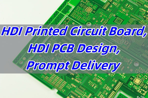
HDI printed circuit board is at the core of today’s compact, powerful, and high-speed electronics. If your product needs faster signals, tighter space, and better reliability, HDI technology is the smart choice.
EBest Circuit (Best Technology) is committed to providing HDI printed circuit board prototypes, HDI PCB design, and assembly to all walks of life. We help clients avoid rework by offering DFM reviews early. With our in-house testing, traceability via MES, and certifications like ISO 13485, IATF 16949, and AS9100D, we meet medical, auto, and aerospace needs. Plus, we keep the consistency of quality and prompt delivery. If any HDI printed circuit board cases need us to help, just kindly contact us at sales@bestpcbs.com anytime.
What is a HDI Printed Circuit Board?
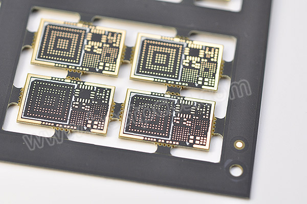
HDI, short for High-Density Interconnect, is a type of PCB that features finer lines and spaces, smaller vias, and higher connection pad density. It’s made for advanced designs where every millimeter matters. Unlike standard boards, it can carry more components in less space, helping devices stay sleek yet powerful.
What is the Difference Between HDI PCB and Normal PCB?
Standard PCBs are good for basic layouts, but HDI PCBs offer more layers and tighter designs. Normal PCBs use through-hole vias. HDI boards use microvias, blind vias, and buried vias. This change cuts noise, boosts speed, and reduces size. For high-frequency or multi-functional applications, HDI outperforms standard boards easily.
What is the HDI Layout?
An HDI layout uses small vias and tight routing to pack more functionality into each layer. Designers need to consider signal integrity, heat paths, and high-speed rules. With fine trace widths below 75μm and via-in-pad structures, HDI layouts allow smartphones, medical tools, and automotive modules to do more in less space.
How Many Layers Can a Printed Circuit Board Have?
In general, PCBs can have 2 to over 20 layers. For HDI printed circuit boards, the layer count often ranges from 4 to 12, depending on how many build-up layers and via combinations are used. Complex HDI stacks with multiple sequential laminations offer unmatched performance in small packages.
How to Do the HDI PCB Design?
Designing HDI requires early coordination with the PCB manufacturer. First, follow the HDI PCB design guide PDF to understand manufacturing limits. Use tools that support blind/buried via planning, differential pair spacing, and impedance control. Simulate DFM early and apply rules like the 3W spacing rule to cut cross-talk. At EBest Circuit (Best Technology), we review your layout with CAM teams early to reduce back-and-forth and shorten design time.
How Does a HDI Printed Circuit Board Work?
HDI boards connect dense components using microvias and stacked structures. Tiny holes link each layer with tight precision, sometimes within 3μm tolerance. Signals travel through controlled-impedance paths, staying clean even at high frequencies. With embedded parts and advanced plating, these boards function faster, cooler, and more reliably.
What Are the Advantages of Printed Circuit Board?
Printed circuit boards give electrical stability, compact form, and ease of mass production. With HDI upgrades, they also give you stronger signal performance, better thermal paths, and increased routing space. You can fit more IOs, more power control, and faster processing—all on a smaller footprint.
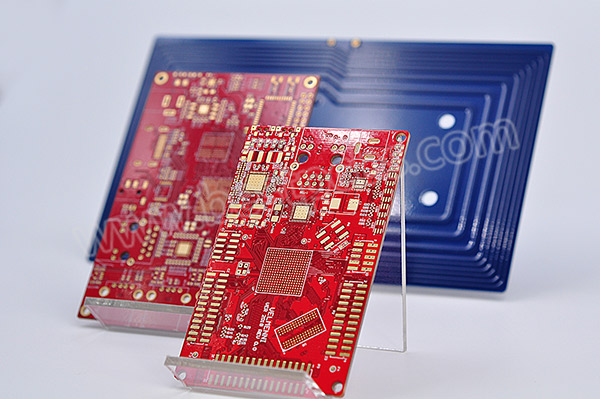
What is HDI Printed Circuit Board Used For?
You’ll find HDI PCBs in smartphones, cameras, medical gear, servers, and automotive radar systems. Anywhere size, speed, and reliability matter, these boards lead the way. They are also essential in HDI electronics like wearables, military tech, and 5G communication.
In summary, choosing an HDI printed circuit board isn’t just a technical decision—it’s a strategic one. Whether you need better signal routing, smaller layouts, or faster thermal relief, HDI gives you an edge. As a tech-driven HDI PCB Manufacturer, EBest Circuit (Best Technology) backs that up with smart design help, better materials, and prompt delivery. A warm welcome to contact us at sales@bestpcbs.com for any HDI PCB design needs.
Tags: HDI PCB Design, HDI Printed Circuit Board, Prompt Delivery