

Need FR4 copper clad board solutions? This guide covers material specs, design optimization, and cost-effective strategies for reliable PCB applications.
EBest Circuit (Best Technology) is your trusted partner for high-quality FR4 copper clad circuit boards, offering flexible prototyping services with 1-piece minimum order to meet diverse project needs. Our advanced manufacturing capabilities allow us to produce various PCB types, from simple single-sided boards to complex multilayer designs, ensuring precision and reliability. With 24-hour rapid prototyping and fast-turnaround delivery, we help you accelerate product development without compromising quality. Whether you need standard FR4 or specialized materials with specific Tg, Dk, or flame-retardant properties, our team delivers tailored solutions. Competitive pricing, strict quality control, and responsive customer support make us the ideal choice for engineers and businesses. Contact us today for a quote and experience seamless PCB production from prototyping to mass production. Let’s turn your designs into reality efficiently!
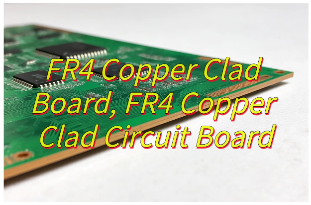
What Is FR4 Copper Clad Board?
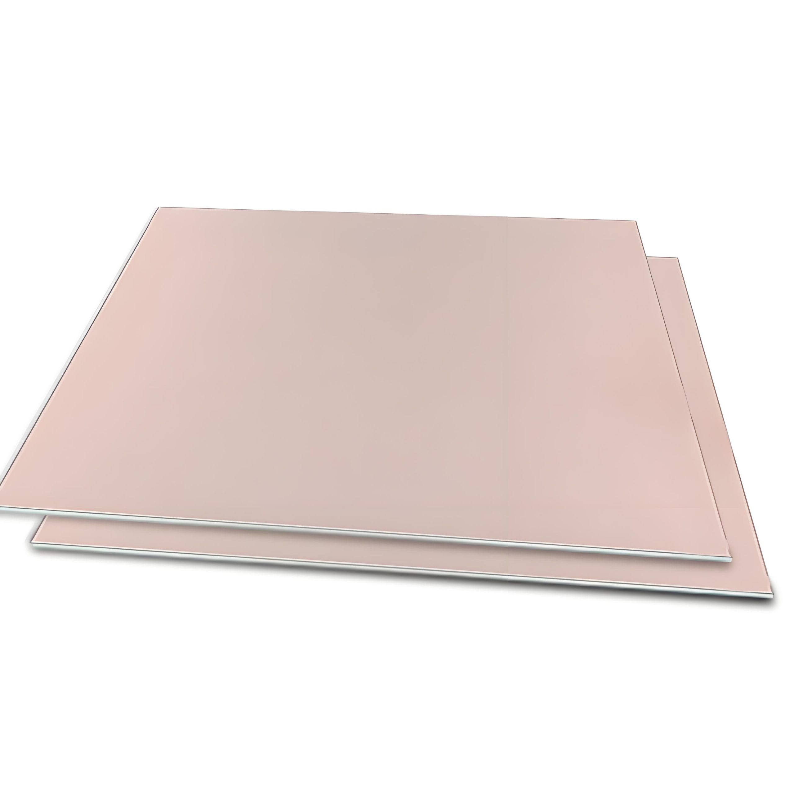
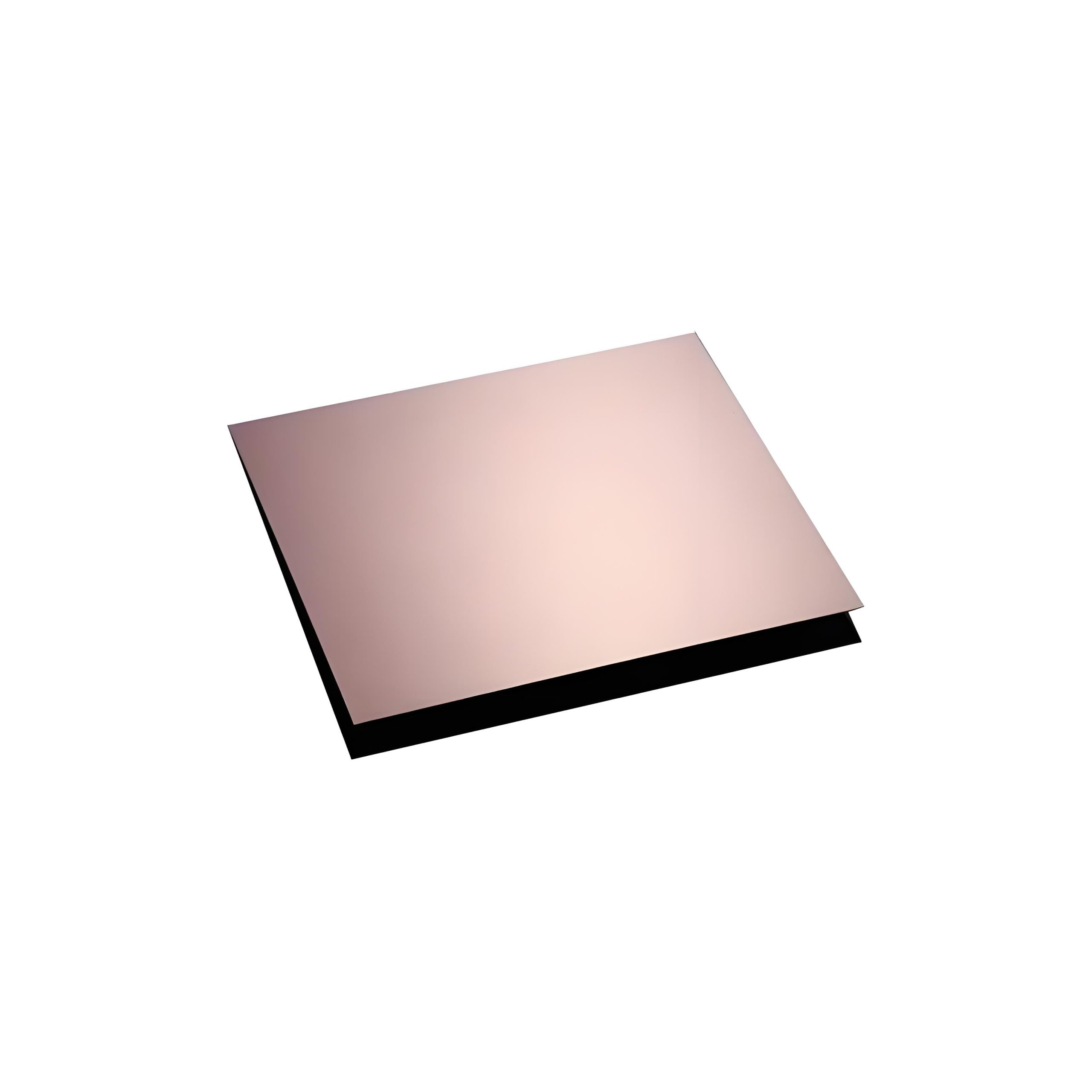
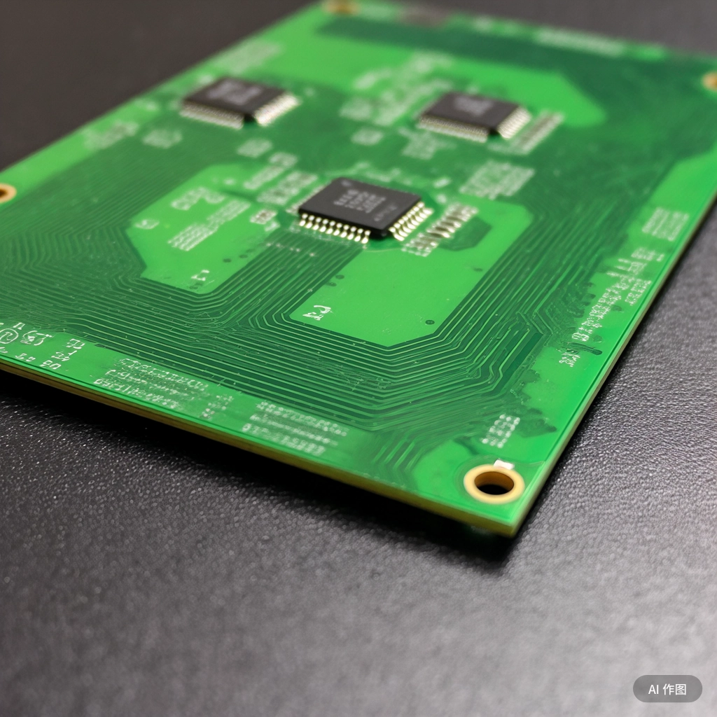
A FR4 copper clad board constitutes the essential base material for fabricating rigid printed circuit boards, comprising a substrate of woven fiberglass cloth impregnated with flame-retardant epoxy resin laminated with conductive copper foil on one or both surfaces. This inherently flame-resistant FR4 substrate provides structural rigidity, electrical insulation, and dimensional stability, while the bonded copper layer establishes the conductive pathways necessary for electronic circuits. During manufacturing, this raw FR4 copper clad board undergoes processes like etching, drilling, and plating to selectively remove copper and define precise circuit patterns, transforming it into a functional FR4 copper clad circuit board. The resultant board supports component assembly and solder connections, leveraging copper’s excellent conductivity alongside FR4’s mechanical durability and thermal resilience for reliable operation across diverse electronic applications ranging from consumer devices to industrial systems. This material combination delivers consistent performance under typical operating conditions.
How thick Is FR4 Copper Clad Board?
The thickness of an FR4 copper clad board varies considerably based on its construction type, core substrate thickness, and copper foil weight. Here’s a practical breakdown for different scenarios:
- Base Laminate Thickness (FR4 Core): The foundation starts with the FR4 substrate itself. Common standard thicknesses for this rigid core material include widely used options like 0.4 mm, 0.6 mm, 0.8 mm, 1.0 mm, 1.2 mm, 1.6 mm (a frequent standard), 2.0 mm, 2.4 mm, and 3.2 mm. Manufacturing tolerances typically fall within ±10% for these values.
- Copper Foil Contribution: Copper thickness, specified by weight (e.g., ounces per square foot), directly adds to the total dimension. Standard weights are 0.5 oz (~17.5 µm), 1.0 oz (~35 µm – most prevalent), and 2.0 oz (~70 µm). Heavy copper options like 3 oz or 4 oz exist for specialized needs. Crucially, this copper thickness applies to each clad side.
- Single-Sided FR4 Copper Clad Board: The overall thickness here combines the core thickness plus the single copper layer. For example, a 1.6 mm core with 1 oz copper results in roughly 1.635 mm total thickness. The copper typically adds a small but measurable increment.
- Double-Sided FR4 Copper Clad Circuit Board: Copper cladding exists on both surfaces. Consequently, the total thickness equals the core thickness plus the combined copper thickness from both sides. Therefore, a 1.6 mm core with 1 oz copper on each side yields approximately 1.67 mm.
- Multi-Layer FR4 Copper Clad Circuit Board: These involve stacking multiple cores and copper layers bonded with prepreg (uncured epoxy-fiberglass). Total thickness depends on the number of layers, individual core thicknesses, prepreg thicknesses, and all copper weights. Furthermore, lamination pressure compresses the layers. A typical 4-layer board might measure between 0.8 mm and 1.6 mm, whereas complex boards with 12 or more layers can reach 3.0 mm or beyond.
What Are Performance Parameters of FR4 Copper Clad Board?
Here are the primary performance parameters defining the functionality and reliability of FR4 copper clad board, commonly grouped by characteristic type:
Electrical Properties
- Dielectric Constant (Dk or ε_r): Measures the substrate’s ability to store electrical energy relative to vacuum. Standard FR4 typically exhibits a Dk between 4.3 and 4.8 at 1 MHz. This value influences signal speed and impedance control.
- Dissipation Factor (Df or tan δ): Indicates inherent signal energy loss as heat within the dielectric material. Lower values are preferable for high-frequency applications. Standard FR4 generally has a Df around 0.020 at 1 MHz.
- Surface and Volume Resistivity: Quantifies the insulating material’s resistance to electrical leakage current flow across its surface or through its bulk, typically exceeding 10⁶ MΩ or 10⁸ MΩ-cm respectively after moisture conditioning.
- Dielectric Strength: Represents the maximum voltage the insulating material can withstand per unit thickness before breakdown occurs, usually measured in kV/mm.
- Copper Resistivity: The inherent resistance of the copper foil itself, crucial for current-carrying capacity and trace heating.
Thermal Properties
- Glass Transition Temperature (TG): The temperature at which the resin transitions from a rigid glassy state to a softer rubbery state. Standard FR4 has a TG typically around 130-140°C, while high-TG variants offer 170°C, 180°C, or higher for improved thermal stability.
- Thermal Decomposition Temperature (Td): The temperature where the material begins to chemically decompose, measured by weight loss. A higher Td indicates better resistance to thermal degradation during soldering.
- Coefficient of Thermal Expansion (CTE): Measures dimensional change per degree of temperature change, both in-plane (x, y) and through-plane (z). Matching CTE between copper and FR4 laminate helps prevent via failure during thermal cycling. Z-axis CTE below TG is particularly important.
- Thermal Conductivity: The material’s ability to conduct heat. FR4 has relatively low thermal conductivity compared to metal-core or ceramic substrates.
Mechanical Properties
- Peel Strength: Measures the adhesion force required to separate the copper foil from the FR4 substrate, typically expressed in N/mm or lb/in. This is vital for solder joint and trace integrity.
- Flexural Strength: Indicates the material’s resistance to bending or breaking under load, relevant for board rigidity and handling during assembly.
- Young’s Modulus (Modulus of Elasticity): Describes the stiffness of the FR4 material under tensile or compressive stress.
- Dimensional Stability: Refers to the laminate’s ability to maintain its size and shape under varying environmental conditions like temperature and humidity, affecting registration accuracy.
Chemical & Environmental Properties
- Flammability Rating: FR4 inherently meets UL94 V-0 (vertical burning test) standards, signifying excellent self-extinguishing properties critical for safety.
- Moisture Absorption: The percentage weight gain after immersion in water under specified conditions. Lower absorption (e.g., <0.1% after 24hrs immersion) enhances reliability in humid environments and prevents issues like conductive anodic filament (CAF) growth or delamination during soldering.
- Chemical Resistance: The ability to withstand exposure to solvents, acids, and alkalis encountered during manufacturing (etching, stripping, plating) and operation.
- Halogen Content: Standard FR4 contains halogens (bromine for flame retardancy). Halogen-free FR4 alternatives exist for environmental compliance and reduced toxicity concerns.
Dimensional & Structural Properties
- Laminate Thickness Tolerance: The allowable variation in the overall thickness of the FR4 Copper Clad Board, typically specified as ±10% or tighter for critical applications.
- Copper Foil Thickness/Weight: Standardized weights (e.g., 0.5 oz, 1 oz, 2 oz) define the thickness of the conductive layer before etching, directly impacting current carrying capacity and trace width requirements.
- Surface Quality: Refers to imperfections like pits, scratches, or voids on the copper or laminate surface affecting manufacturability.
- Prepreg Compatibility: For multilayer FR4 Copper Clad Circuit Board fabrication, the resin flow and bonding characteristics of the prepreg used with the core laminates are essential for layer adhesion and void minimization.
What Is Function of FR4 Copper Clad Circuit Board?
Function of FR4 copper clad circuit board:
- Provides Structural Foundation: Creates a rigid, stable platform on which all electronic components can be securely mounted and interconnected, ensuring the physical integrity of the entire assembly during manufacture, handling, and operation. This structural rigidity protects delicate components from damage.
- Offers Electrical Insulation: The FR4 substrate acts as a highly effective electrical insulator between conductive copper traces and layers. This prevents unintended short circuits and allows complex circuits with closely spaced conductors to function reliably, even at typical operating voltages.
- Forms Conductive Pathways: The laminated copper foil allows precise etching of custom electrical pathways (traces or tracks). These pathways carry signals and power efficiently between components like resistors, capacitors, integrated circuits, and connectors, enabling the designed circuit functionality.
- Facilitates Component Attachment: Provides durable, solderable copper surfaces (pads and lands) where electronic components are securely attached using soldering processes. Strong copper adhesion ensures stable mechanical and electrical connections throughout the product’s lifespan.
- Enables Multi-Layer Design: Allows construction of complex circuits by stacking multiple layers of etched copper and insulating FR4 core/prepreg. This is vital for modern, dense electronics, saving significant space compared to single-layer solutions while maintaining signal separation and integrity between layers. Internal planes can also distribute power and ground efficiently.
- Manages Heat Dissipation: While FR4 itself has limited thermal conductivity, the embedded copper planes and traces help distribute and dissipate heat generated by active components across the board surface, preventing localized overheating and improving overall thermal performance and component longevity.
- Ensures Signal Integrity: Offers predictable electrical properties (Dielectric Constant, Dissipation Factor) that designers rely on to control impedance and minimize signal loss or distortion, especially for digital and moderate-speed analog signals. Controlled impedance traces are achievable for common applications.
- Provides Environmental Protection: The FR4 material exhibits excellent resistance to moisture, many chemicals, and high temperatures encountered during soldering and operation. Its inherent flame retardancy (UL94 V-0) enhances safety by resisting ignition and limiting flame spread.
- Supports Manufacturing Efficiency: The combination of FR4 and copper clad is highly compatible with standard, cost-effective PCB fabrication processes (drilling, routing, plating, etching, soldering). This drives down production costs while ensuring consistent quality and reliability in high-volume manufacturing.
- Enhances Design Versatility: Available in a wide range of thicknesses, copper weights, and specific grades (like high TG), these boards offer flexibility. Designers can select the optimal combination for diverse applications, from simple consumer gadgets to demanding industrial controls, balancing cost, performance, and durability.
- Ensures Long-Term Reliability: Meets stringent requirements for thermal cycling resistance, dimensional stability, and resistance to environmental factors like humidity. This translates directly to durable end products that perform consistently even under challenging conditions, reducing warranty claims and maintenance costs.
- Provides Grounding and Shielding: Large copper areas serve as effective ground planes, reducing electromagnetic interference (EMI) and noise susceptibility. Copper layers can also function as shielding planes, containing electromagnetic emissions and protecting sensitive circuit sections.
How to Optimize FR4 Copper Clad Circuit Board Layout for Signal Integrity?
Below are practical strategies about optimize FR4 copper clad circuit board layout for signal integrity:
- Maintain Consistent Impedance Profiles: Ensure uniform trace geometries (width, thickness, dielectric spacing) to stabilize impedance (e.g., 50 Ω for RF lines). Use backdrilled vias or blind vias to minimize stub effects in high-speed channels. This prevents reflections in interfaces like HDMI or USB 3.0, ensuring error-free data transmission.
- Route Differential Pairs with Precision: Match trace lengths and maintain 3–5× trace-width spacing between pairs to balance skew and reduce crosstalk. For applications like PCIe or MIPI, this approach preserves signal quality at multi-gigabit rates.
- Design Layer Stack-Ups Strategically: Assign high-speed signal layers between contiguous ground planes. In 4-layer boards, prioritize Layer 1 for critical traces with Layer 2 as a ground reference. This shielding reduces EMI and loop inductance, benefiting noise-sensitive analog circuits.
- Isolate Noisy and Sensitive Circuits: Separate switching regulators, clocks, or RF transmitters from analog sections by at least 3× trace widths. Use inner layers with guard rings for low-noise analog traces, such as sensor interfaces or audio pathways.
- Optimize Decoupling Capacitor Placement: Place 0.1 µF and 10 µF capacitors within 2 mm of IC power pins. Use X7R or NP0 dielectric capacitors for stable performance across temperatures. This stabilizes power delivery to processors, preventing glitches in memory or communication modules.
- Avoid Sharp Bends and Minimize Stubs: Route traces with 45° angles or filleted corners to reduce impedance discontinuities. Trim via stubs shorter than 1/10th the signal wavelength (e.g., < 3 mm for 10 Gbps signals).
- Leverage Simulation Early in the Design Cycle: Use pre-layout SI tools to model reflections, crosstalk, and power integrity. Post-layout eye-diagram analysis ensures compliance with standards like IEEE 802.3. Early simulations catch issues before fabrication, saving rework costs.
- Collaborate with Manufacturers on DFM Rules: Document trace/space tolerances, via specifications, and material requirements clearly. Align with fabricators’ capabilities to avoid misinterpretations that could degrade signal integrity.
How to Choose the Right FR4 Grade for Your Design to Avoid Performance Issues?
Match Thermal Properties to Your Application
- Standard Use: For everyday devices like toys or basic controls, FR4 with Tg 130–150°C works well.
- High Heat: Automotive or power electronics need high-Tg FR4 (170–190°C) to handle lead-free soldering and thermal cycling.
- Extreme Conditions: For harsh environments, pick materials with Td above 300°C to avoid delamination.
Align Signal Needs with Dielectric Properties
- Low-Speed Circuits: Digital designs under 1 GHz can use standard FR4 (Dk 4.0–4.7, Df 0.01–0.03).
- Mid-Range Frequencies: For 1–10 GHz (e.g., Wi-Fi), opt for FR4 with lower Dk (3.5–4.0) and Df (<0.008) to cut losses.
- High-Frequency Designs: Above 10 GHz? Combine FR4 with low-loss materials like PTFE for better performance.
Check Mechanical Requirements
- Rigid Designs: Standard FR4’s strength (300–500 MPa) suits enclosures or fixtures.
- Flexible Needs: Use modified FR4 for flex-to-install applications to prevent cracking.
- Multi-Layer Boards: Match CTE across layers to avoid warpage during thermal changes.
Consider Environmental Factors
- Outdoor Use: Choose FR4 with low moisture absorption and UV coatings for durability.
- Chemical Exposure: Opt for epoxy blends resistant to solvents or acids.
Weigh Cost vs. Performance
- Prototypes: Standard FR4 saves money for initial testing.
- Production Runs: Premium grades reduce field failures in mass-produced items.
Involve Your Manufacturer Early
- Share thermal, electrical, and mechanical specs with your PCB fabricator.
- Test material samples to confirm properties like dielectric constant and peel strength.
Verify Regulatory Compliance
- Ensure FR4 meets UL94 V-0 for consumer safety.
- For medical or automotive projects, check industry standards like ISO 13485.
Plan for Upgrades
- If your design might scale to higher speeds or temps, pick FR4 with headroom (e.g., mid-Tg) to avoid future redesigns.
How Reliable Is FR4 Copper Clad Circuit Board Assembly Under Humidity Testing?
Here’s how to ensure FR4 copper clad circuit board stay reliable through humidity testing and real-world exposure:
- Choose Moisture-Resistant FR4 Materials: Pick FR4 grades with resin systems that resist water absorption. Look for materials absorbing <0.2% moisture—this cuts risks of delamination and electrical leaks. Ideal for outdoor gear like LED lights or marine sensors.
- Add Protective Coatings: After assembly, apply acrylic, silicone, or urethane coatings to block moisture. Parylene works best for harsh environments. These layers prevent corrosion and short circuits in humid places like bathrooms or greenhouses.
- Design for Water Runoff: Shape boards with sloped edges and avoid recessed areas where water could pool. Proper drainage matters for devices exposed to rain or dew, such as smart irrigation controls.
- Use Durable Surface Finishes: Prioritize ENIG (Electroless Nickel Immersion Gold) or immersion silver instead of HASL. These finishes resist oxidation better, keeping solder joints intact in damp conditions—perfect for HVAC systems or outdoor appliances.
- Keep Copper Away From Edges: Maintain ≥0.5 mm space between traces and board edges. This prevents moisture from wicking into fibers, reducing edge plating issues in boards used near water, like those in kitchens or boats.
- Seal Vias and Holes: Fill plated holes with resin or cap them with copper to block moisture. This stops corrosion in automotive sensors or drones operating in wet conditions.
- Dry Boards Before Assembly: Store bare boards in sealed bags with desiccant. Bake them at 105–125°C for 4–6 hours to remove absorbed moisture. This prevents soldering issues like popcorning, common in humid factories.
- Ensure Proper Ventilation: Add ventilation holes or heat sinks to prevent condensation inside enclosures. Critical for devices like ATMs or kiosks in damp locations.
- Test Under Extreme Conditions: Run 85°C/85% RH tests for 1,000+ hours to simulate years of use. Track insulation resistance and leakage to spot problems early.
- Pick RoHS-Compliant Laminates: Use halogen-free FR4 (IEC 61249-2-21 compliant) to reduce hygroscopicity. These materials resist blooming and delamination better than traditional options in damp settings.
How to Balance FR4 Copper Clad Circuit Board Performance and Cost?
Right-Size Material Grade
- For basic consumer devices (e.g., toys, simple controls), standard FR4 with Tg 130–150°C and mid-range dielectric properties (Dk 4.0–4.7) offers sufficient performance at low cost.
- Reserve high-Tg, low-loss, or halogen-free FR4 variants for applications requiring thermal stability, high-speed signals, or regulatory compliance (e.g., automotive, industrial).
Optimize Layer Count and Stack-Up
- Use 2-layer boards for low-density designs (e.g., LED drivers) to minimize fabrication costs.
- For multi-layer boards, adopt a 4-layer stack-up with dedicated power/ground planes only if signal integrity or EMI control is essential. Avoid unnecessary layers that add expense.
Simplify Trace Routing and Via Usage
- Route high-speed signals in inner layers with adjacent ground planes to reduce EMI without adding complex impedance control layers.
- Limit via counts by using through-hole components sparingly and optimizing footprint placement. Blind/buried vias should be used only for density-critical designs (e.g., smartphones).
Standardize Component Placement
- Use surface-mount devices (SMDs) instead of through-hole components to reduce drilling costs and enable automated assembly.
- Group similar components (e.g., capacitors, resistors) to streamline pick-and-place processes.
Leverage Panelization and Volume Discounts. - Panelize multiple boards into a single array to reduce per-unit handling costs.
- Negotiate bulk pricing with fabricators for orders exceeding 1,000 units, as FR4’s economies of scale become significant at higher volumes.
Apply Cost-Effective Surface Finishes
- Use HASL (Hot Air Solder Leveling) for general-purpose boards due to its low cost and adequate performance.
- Reserve ENIG (Electroless Nickel Immersion Gold) for applications requiring fine-pitch SMDs or aluminum wire bonding, as it adds 10–15% to assembly costs.
Design for Manufacturability (DFM)
- Maintain ≥0.1 mm trace/space clearance and ≥0.3 mm drill-to-copper spacing to avoid yield losses from etching or drilling errors.
- Avoid sharp angles or acute traces that complicate etching and increase scrap rates.
Reuse Test Fixtures and Jigs
- For recurring designs, invest in reusable flying probe or ICT (In-Circuit Test) fixtures to amortize testing costs over multiple batches.
Conclusion
FR4 copper clad boards offer balanced electrical, thermal, and mechanical properties for diverse applications. From standard single-sided designs to complex multilayer circuits, understanding thickness options (like 1.6mm common variants), performance parameters, and layout optimization techniques ensures project success. Rigorous humidity testing proves their reliability in harsh environments, while strategic material selection avoids over-engineering costs. For tailored FR4 solutions with competitive pricing, contact EBest Circuit (Best Technology) to discuss your project’s specific copper weight, dielectric requirements, and volume needs. Their expertise in FR4-grade matching and fabrication support streamlines your PCB development cycle.