

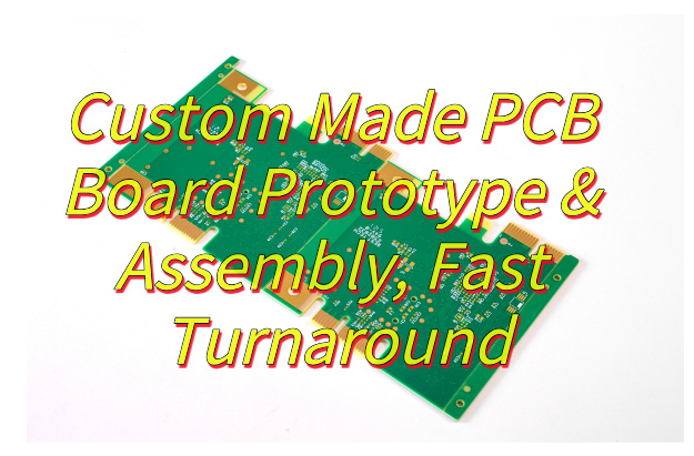
Looking for high performance custom made PCB board solutions for your project? This guide reveals how tailored designs, rapid prototyping, and precision assembly deliver optimized performance without compromising speed or reliability.
EBest Circuit (Best Technology) is your trusted partner for high-quality custom made PCB boards, delivering industry-leading speed and reliability for both single-layer PCB prototypes and complex multilayer boards up to 32 layers.. With our 24-hour rapid prototyping service, backed by a 99.1% on-time delivery rate, we ensure your projects stay on schedule without compromising quality. Our boards undergo 12-layer AOI inspection and impedance testing, achieving a <0.05% defect rate for unmatched performance. We offer transparent pricing with no hidden fees, saving clients 15-30% compared to competitors, and support 1-piece minimum orders to reduce prototyping costs. With 10+ years of expertise in aerospace and medical-grade PCBs, we handle complex designs with ±0.02mm trace accuracy. Over 10,000 successful prototypes delivered to global clients prove our capability to meet tight deadlines while maintaining precision. Contact us today for a free DFM analysis within 2 hours and experience faster, smarter PCB solutions tailored to your needs: sales@bestpcbs.com.
What Is Custom Made PCB Board?
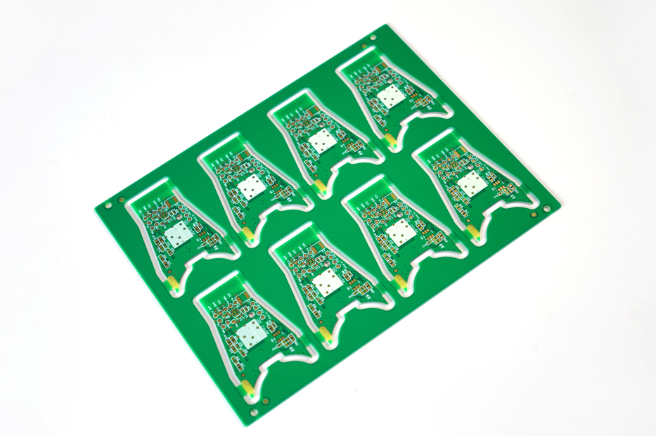
A custom made PCB board is a printed circuit board specifically designed to meet unique technical requirements, differing from standard off-the-shelf solutions. These boards are engineered with particular layer counts, materials, and circuitry patterns to serve specialized applications while maintaining reliable performance. When ordering custom PCB board prototypes, engineers benefit from tailored solutions that precisely match their project specifications, whether for compact wearable devices or complex industrial systems. The assembly process for custom made PCB board products emphasizes fast turnaround times without compromising quality, using automated optical inspection and precision soldering techniques to ensure each unit meets design intent. This approach allows for rapid iteration during development cycles while maintaining production-grade reliability.
Why Choose Custom Made PCB Board?
Reasons why choose custom made PCB board:
- Precision Design Matching: Custom made PCB boards are engineered to your exact schematics, ensuring every trace width, layer stackup, and component placement aligns with your project’s electrical and mechanical needs.
- Accelerated Prototyping: With fast-turnaround services, these boards enable rapid design validation, often delivering functional prototypes within days to streamline product development cycles.
- Material Flexibility: Choose from specialized substrates like high-frequency laminates or flexible polymers tailored to your application’s thermal, mechanical, or signal integrity demands.
- Scalable Production: Seamlessly transition from prototype to mass production while maintaining consistent quality, thanks to standardized manufacturing processes optimized for your design.
- Cost-Efficient Optimization: Reduce wasted board area through panelization strategies and eliminate unnecessary features found in generic PCBs, lowering per-unit costs at higher volumes.
- Reliability Enhancements: Custom designs incorporate proper clearances, impedance control, and testing points from the outset, minimizing field failures and rework expenses.
- Integration Support: Accommodate mixed-technology assemblies (SMT/THT) and complex components like BGAs or QFNs without compromising assembly speed or yield rates.
What Customization Options Can Custom PCB Boards Provide?
Customization options for custom PCB board:
Material Versatility
- FR-4: A standard choice for general-purpose electronics, offering a balance of affordability and mechanical robustness.
- Metal Core PCBs (MCPCB): Optimize thermal management for high-power applications like LED lighting or motor drivers, using aluminum or copper cores to dissipate heat efficiently.
- High-Frequency Laminates: Essential for RF, microwave, or high-speed digital circuits, these materials (e.g., Rogers or PTFE) minimize signal loss and maintain impedance stability.
Layer Configuration
- Single-Layer Boards: Simplify low-density designs, such as basic sensors or single-function controllers.
- Double-Sided Boards: Maximize component density and routing flexibility for moderate-complexity projects.
- Multilayer Boards (4+ Layers): Enable advanced routing for high-speed signals, power distribution, and electromagnetic interference (EMI) reduction through dedicated power/ground planes.
Form Factor Flexibility
- Custom Panel Sizes: Align board dimensions with enclosure requirements to minimize material waste and assembly costs.
- Contour Cutting: Create non-rectangular boards using CNC routing or scoring, ideal for wearables, drones, or ergonomic devices.
Surface Finish Selection
- HASL (Hot Air Solder Leveling): A cost-effective option for through-hole components, though less suitable for fine-pitch surface-mount parts.
- ENIG (Electroless Nickel Immersion Gold): Provides a flat, corrosion-resistant surface, perfect for gold wire bonding or fine-pitch SMT assembly.
- OSP (Organic Solderability Preservative): An eco-friendly, short-term storage solution for prototypes needing quick assembly.
Specialized Manufacturing Techniques
- Flex-Rigid Boards: Combine rigid and flexible substrates to create 3D assemblies, reducing weight and space in medical or consumer electronics.
- Heavy Copper (≥3 oz/ft²): Withstand high currents in power supplies or electric vehicle components without overheating.
- Edge Plating: Add conductive edges for RF shielding, board-to-board connectors, or power distribution in dense systems.
End-to-End Assembly Services
- Turnkey Assembly: Manage component sourcing, stencil printing, and reflow soldering under one roof to reduce lead times.
- Conformal Coating: Apply protective layers to resist moisture, dust, and vibration in harsh environments.
How to Achieve Custom Made PCB Board Fast Turnaround Prototyping?
Here are actionable measures to achieve fast turnaround for custom PCB board prototyping:
Streamline design file preparation:
- Submit complete and error-free Gerber files, bills of materials (BOMs), and assembly drawings.
- Use standardized layer stack-ups and avoid non-standard hole sizes or trace spacings that may require special tooling.
- Validate designs using online DRC (Design Rule Check) tools to catch issues early.
Select manufacturers with dedicated rapid-prototyping lines:
- Prioritize suppliers using automated optical inspection (AOI) and automated drilling machines, as these technologies reduce human intervention and accelerate production steps.
- Confirm their ability to handle small-batch orders without lengthy setup times.
Leverage cloud-based collaboration platforms:
- Share real-time design updates and feedback through secure portals, minimizing back-and-forth emails.
- Some platforms offer instant quoting and order tracking, keeping projects on schedule.
Utilize pre-approved material libraries:
- Choose substrates, solder masks, and surface finishes from the manufacturer’s existing stock to avoid sourcing delays. For specialized needs, confirm material lead times upfront.
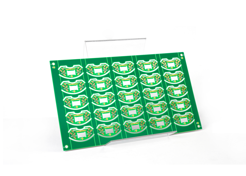
Adopt panelization for small boards:
- Combining multiple copies of a PCB into a single panel reduces handling time during fabrication and assembly.
- Ensure panel layouts include tooling holes and fiducial markers for automated equipment.
Prioritize clear communication channels:
- Designate a single point of contact at the manufacturer for queries and approvals.
- Promptly address any questions about design intent or specifications to prevent bottlenecks.
Explore expedited shipping and logistics:
- Prioritize overnight delivery or priority courier services for finished prototypes. Some manufacturers partner with global logistics providers to ensure timely customs clearance and doorstep delivery.
Plan for iterative testing in parallel:
- While awaiting the first prototype, prepare test jigs and software scripts to validate functionality immediately upon receipt. This proactive approach reduces idle time between revisions.
Can Custom Made PCB Prototyping Ensure Pad and Trace Accuracy for Reliable Testing?
Yes, custom PCB prototyping can ensure pad and accuracy for reliable testing through several key measures that directly benefit your product development and quality assurance efforts. Here’s how:
- Advanced Manufacturing Technologies: Utilizing laser drilling and optical positioning systems achieves micron-level precision in creating vias, pads, and traces. This consistency ensures that test probes make reliable contact during in-circuit testing (ICT) or flying probe tests, minimizing false failures or misdiagnoses.
- Design Rule Checks (DRC): Before production, DRC software automatically verifies trace widths, spacing, and pad dimensions against manufacturing capabilities. This process eliminates potential issues such as acid traps or insufficient annular rings, which could compromise testability and product reliability.
- Impedance Control: Custom PCBs allow precise tuning of trace geometry and dielectric materials to match specific impedance requirements. This accuracy is crucial for maintaining signal integrity in high-speed applications, ensuring that test results accurately reflect the board’s performance.
- Material Consistency: High-quality laminates with stable thermal expansion coefficients are used to prevent pad lifting or trace misalignment during thermal cycling tests. This reliability is particularly important for applications in extreme environments, such as automotive or aerospace sectors.
- Dedicated Prototype Production Lines: Many manufacturers employ automated equipment reserved specifically for prototype production. This setup minimizes setup changes and human intervention, ensuring consistent quality and precision in each board produced.
- Impedance-Controlled Testing: Post-production tests like time-domain reflectometry (TDR) verify trace impedance. Any deviations from specifications trigger immediate adjustments to the manufacturing process, ensuring subsequent boards meet the required standards.
- Detailed Documentation: Manufacturers provide comprehensive inspection reports detailing pad dimensions, solder mask alignment, and trace spacing. This data aids engineers in isolating testing issues to design flaws rather than manufacturing inconsistencies.
- Iterative Refinement: Rapid prototyping allows quick adjustments to pad sizes or trace routing based on test feedback. This agility reduces the risk of systemic errors in later production stages, accelerating time-to-market.
Can Fast Turnaround Prototypes Meet Deadlines Without Quality Compromise?
Yes, fast turnaround PCB prototypes can meet deadlines without compromising quality through a combination of streamlined processes, advanced technologies, and rigorous quality controls. Below are the factors that ensure both speed and reliability:
- Automated Design Verification: Manufacturers use automated tools to check for design errors, such as trace spacing violations or incorrect drill sizes, before production begins. This eliminates rework caused by avoidable mistakes and accelerates the validation phase.
- Parallel Workflows: Prototyping and testing phases overlap with design iterations. While engineers refine a design, manufacturers prepare materials and tooling, reducing idle time between stages.
- Optimized Material Sourcing: Pre-negotiated contracts with suppliers ensure quick access to standard substrates, laminates, and solder masks. This avoids delays from custom material orders while maintaining material integrity.
- Dedicated Rapid-Production Lines: Separate production lines equipped with high-speed drills, laser etchers, and automated optical inspection (AOI) systems prioritize prototypes. These lines minimize setup times and focus solely on quick-turn orders.
- In-Process Quality Checks: Real-time monitoring tools, such as electrical test (ET) and impedance testing, occur during fabrication. Early detection of issues like trace shorts or impedance mismatches prevents delays from late-stage failures.
- Experienced Engineering Support: Technical teams review designs for manufacturability (DFM) and suggest adjustments to balance speed and quality. For example, recommending standard hole sizes or panelization to reduce complexity.
- Priority Shipping and Logistics: Manufacturers partner with logistics providers to expedite shipments. Overnight delivery or express courier services ensure prototypes arrive on schedule, even for urgent international orders.
- Transparent Communication: Regular updates via email, SMS, or dashboards keep clients informed about production status. Proactive alerts about potential delays allow teams to adjust timelines or priorities dynamically.
How Does Custom Made PCB Design Complexity Impact Assembly?
Here are how custom made PCB design complexity impact assembly:
High Layer Counts and Stack-Up Complexity:
- Impact: Multi-layer boards with intricate stack-ups require precise registration during drilling and lamination. Misalignment can cause via breaks or impedance mismatches.
- Solution: Use design software to simulate layer alignment and share stack-up details with assemblers upfront. Prioritize semi-cured laminate (prepreg) sheets with tight thickness tolerances to minimize variability.
Fine-Pitch Components and Micro-BGA Packages
- Impact: Tiny component leads and dense ball grid arrays (BGAs) demand high-accuracy placement tools. Manual soldering becomes impractical, increasing rework risks.
- Solution: Partner with assemblers using advanced pick-and-place machines with sub-50-micron accuracy. Incorporate fiducial markers and solder paste inspection (SPI) to ensure precise alignment.
Mixed-Technology Integration
- Impact: Combining through-hole, SMT, and hybrid components complicates assembly workflows, requiring multiple soldering processes.
- Solution: Group components by technology in the design phase. Use wave soldering for through-hole parts and reflow ovens for SMT components, with clear panelization to separate zones.
High-Speed Signal Requirements
- Impact: Controlled impedance traces and differential pairs need specialized soldering to avoid skew or signal loss.
- Solution: Specify low-residue no-clean flux and nitrogen-reflow atmospheres to reduce oxidation. Validate with time-domain reflectometry (TDR) post-assembly.
Rigid-Flex and 3D Designs
- Impact: Bends, folds, and multi-section boards challenge automated assembly equipment.
- Solution: Provide 3D STEP models to assemblers and use flexible circuit carriers for rigid-flex panels. Add stiffeners to critical areas to maintain planarity during soldering.
High Component Density
- Impact: Crowded boards increase solder bridging risks and reduce inspection accessibility.
- Solution: Apply solder mask dams between pads and use smaller solder paste stencils (e.g., 0.1mm aperture). Automated optical inspection (AOI) with multi-angle lighting detects bridges post-reflow.
Specialty Materials and Finishes
- Impact: Exotic substrates (e.g., PTFE, ceramic) or finishes (e.g., ENEPIG) may require non-standard solder profiles or handling.
- Solution: Share material datasheets with assemblers early. Conduct trial runs to calibrate reflow ovens and ensure compatibility with stencils and fluxes.
Thermal Management Features
- Impact: Heat sinks, thermal vias, and metal-core PCBs complicate assembly due to weight and warpage risks.
- Solution: Use staggered vias to distribute heat evenly and pre-bake boards to reduce moisture. Secure heavy components with adhesive during reflow to prevent shifting.
How to Avoid Assembly Errors with Complex Multilayer Custom Made PCBs?
Below are ways about how to avoid assembly errors with complex multilayer custom made PCBs:
- Design for Assembly (DFA) Principles: Simplify component placement by grouping parts by height and function. Use standardized footprints and avoid overly tight tolerances unless essential. Include 3D models in design files to help assemblers visualize component interactions.
- Advanced Layer Alignment Techniques: Incorporate fiducial markers on every layer and use laser-drilled alignment holes to ensure precise stacking during lamination. Share Gerber files with assemblers early to validate layer registration.
- Optimized Solder Paste Stencils: Use laser-cut stainless-steel stencils with nano-coating to prevent solder paste smearing. For fine-pitch areas, reduce stencil aperture sizes by 10–20% to minimize solder bridging.
- Automated Inspection Protocols: Deploy AOI (Automated Optical Inspection) systems with multi-angle lighting to detect lifted pads, tombstoned components, or insufficient solder. Integrate X-ray inspection for buried vias and BGA joints.
- Controlled Impedance Verification: Include test coupons on the PCB panel for impedance measurements. Validate results against design specifications using TDR (Time-Domain Reflectometry) before and after assembly.
- Thermal Management During Soldering: Use nitrogen-reflow ovens to reduce oxidation and improve solder wetting. For heavy components, apply adhesive dots to secure parts during reflow and prevent tombstoning.
- Panelization and Depanelizing Strategies: Design breakaway tabs with V-scoring to minimize stress during depanelization. Avoid placing surface-mount components within 2mm of tab edges to prevent damage.
- Collaborative DFM Reviews: Engage assemblers in pre-production meetings to review stack-ups, material choices, and component placements. Address concerns like via-in-pad plating or blind-via accessibility upfront.
Conclusion
In conclusion, for precision-driven electronics, custom made PCB boards deliver solutions from prototyping to mass production. Whether rigid-flexible designs, multilayer configurations, or rapid-turn prototypes, an experienced manufacturer ensures trace accuracy, testing reliability, and on-time delivery without quality trade-offs. Advanced DFM checks and automated assembly minimize errors in complex layouts. Leverage customized materials, layer stacks, and finishes to meet exact specifications. Contact us for fast-turn PCB solutions now: sales@bestpcbs.com.
Tags: Custom Made PCB Board