

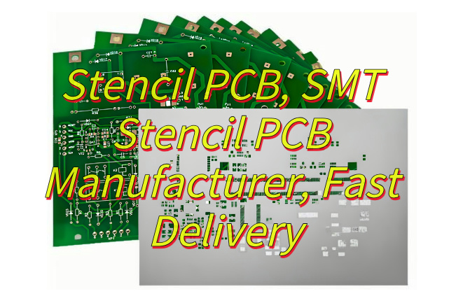
Seeking for stencil PCB solution? Explore its material, type, thickness, design and manufacturing processes, cost reduction and manufacturer selection tips.
EBest Circuit (Best Technology) is a leading SMT stencil PCB manufacturer renowned for fast delivery, precision engineering, and cost-effective solutions. We specialize in high-performance laser-cut stencils, including electropolished, nano-coated, and electroformed options, ensuring optimal solder paste release for flawless SMT assembly. Our 24-48 hour rapid turnaround sets us apart, enabling clients to accelerate production without compromising quality. With ISO-certified manufacturing, ±15μm tolerance control, and strict DFM checks, we guarantee zero-defect stencils tailored to your exact specifications. Backed by global logistics partnerships (DHL/FedEx), we ship worldwide swiftly, minimizing downtime for time-sensitive projects. Whether prototyping or mass production, we offer competitive pricing, no MOQ restrictions, and 24/7 technical support—making us the ideal partner for PCB assemblers seeking speed, reliability, and affordability. Contact us today for a quick quote and experience seamless production with every order: sales@bestpcbs.com.
What Is Stencil PCB?
A stencil PCB, in essence, is a crucial component in the surface – mount technology (SMT) process. It serves as a precise template that enables the accurate deposition of solder paste or other materials onto specific areas of a printed circuit board (PCB). This stencil is designed with carefully crafted apertures that align precisely with the pads on the PCB where components are to be mounted. By using a stencil PCB, the process of applying solder paste becomes highly controlled, reducing the risk of misapplication, solder bridges, and other soldering defects. This precision is vital for ensuring the reliable electrical and mechanical connections between components and the PCB, which is fundamental for the proper functioning of electronic devices.
What Is Material of Stencil PCB?
Material of stencil PCB:
- Stainless Steel: A common stencil PCB material. It’s durable, dimensionally stable, withstands solder paste printing stress, and its smooth surface enables easy solder paste release.
- Nickel – Plated Steel: Adds corrosion resistance. Ideal for moist or corrosive environments, and the nickel layer increases hardness and lifespan.
- Aluminum: Lighter than steel, cost – effective for weight – sensitive applications like portable devices. But it’s less rigid, requiring careful handling, suitable for less demanding uses.
- Polymer – Based Materials: Some stencils use polymers with specific properties, like flexibility. Useful for non – planar surfaces, though less precise than metal in high – density applications.
- Titanium: High strength – to – weight ratio, excellent corrosion resistance. More expensive, but suitable for high – end applications needing extreme durability and harsh environment resistance.
What Are Types of Stencil PCB?
Types of Stencil PCB:
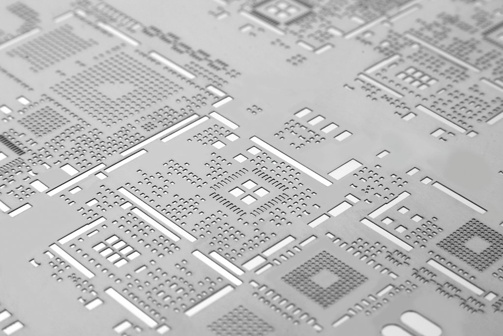
- Laser Cut Stencils: These stencils are created using a laser to precisely cut the apertures in the stencil material, usually stainless steel. Laser cut stencils offer high precision, with the ability to create very fine and complex aperture shapes. They are suitable for high – density SMT applications where tight tolerances are required.
- Electroformed Stencils: Electroforming involves depositing metal onto a patterned mandrel. Electroformed stencils can have extremely smooth sidewalls in the apertures, which promotes better solder paste release. They are often used in applications where high – quality solder paste deposition is crucial, such as in the assembly of fine – pitch components.
- Etched Stencils: Etched stencils are made by chemically etching away the unwanted areas of the stencil material. This method can be used for both simple and moderately complex stencil designs. Etched stencils are a cost – effective option for lower – volume production runs or applications where the precision requirements are not as stringent as in high – end electronics manufacturing.
- Composite Stencils: These stencils combine different materials or manufacturing techniques to achieve specific properties. For example, a composite stencil might have a stainless – steel base with a polymer coating on the surface that comes into contact with the solder paste. The polymer coating can improve the release characteristics of the solder paste while the steel base provides the necessary rigidity.
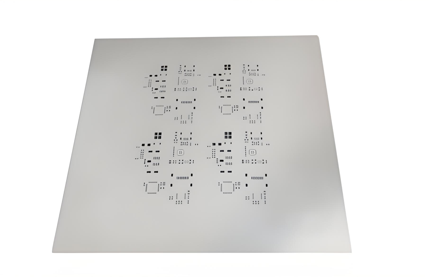
- Multilevel Stencils: In some advanced SMT applications, where components with different heights or solder requirements are present on the same PCB, multilevel stencils are used. These stencils have different levels of apertures, allowing for the application of different amounts or types of solder paste in different areas of the PCB.
How to Choose PCB Stencil Thickness?
PCB stencil thickness selection is component – size dependent:
- Large components: For power components (e.g., large capacitors, inductors) with large pads, use 0.15 – 0.3 mm thick stencils to deposit more solder paste.
- Small components: Fine – pitch components (e.g., 0.4 mm pitch QFP) require 0.08 – 0.12 mm thin stencils to prevent solder bridging.
- Mixed assemblies: In PCBs with both large and small components, consider stepped stencils or laser – cut profiles to optimize paste deposition.
- Solder paste type: Water – soluble pastes may require thinner stencils compared to no – clean pastes to avoid residue issues.
- Printing process: High – precision printers can handle thinner stencils, enabling more accurate paste deposition.
- Board complexity: Dense boards with many components benefit from thinner stencils to minimize solder volume and reduce short – circuit risks.
- Assembly yield: Test different stencil thicknesses on prototypes to find the optimal balance for maximum assembly success rate.
How to Design PCB Stencil?
Here are processes about how to design PCB stencil:
- Understand the PCB Layout: Thoroughly review the PCB layout, including the location, size, and shape of all components and their pads. This understanding is fundamental as it determines the placement and dimensions of the stencil apertures.
- Determine Aperture Dimensions: Calculate the appropriate size of the apertures based on the component pad size. In general, the aperture size should be slightly smaller than the pad size to ensure proper solder paste deposition without excessive spread. For example, for a rectangular pad, the aperture dimensions might be reduced by 10 – 20% on each side.
- Aperture Shape Design: Select the appropriate aperture shape. While rectangular and circular shapes are common, more complex shapes like oval or custom – designed shapes may be necessary for some components to optimize solder paste deposition. For example, for odd – shaped pads or components with specific solder requirements, custom – shaped apertures can be designed.
- Account for Component Clearance: Ensure that there is sufficient clearance between the stencil apertures and any surrounding components or features on the PCB. This prevents interference during the solder paste printing process and reduces the risk of misapplication.
- Consider Solder Paste Volume: Calculate the required volume of solder paste for each component based on its size and the type of connection (e.g., through – hole or surface – mount). Adjust the aperture dimensions and stencil thickness accordingly to achieve the correct solder paste volume.
- Stencil Frame Design: Design a sturdy stencil frame that can hold the stencil material firmly in place during the printing process. The frame should be easy to mount and demount from the printing equipment.
- Marking and Identification: Add clear markings and identification on the stencil, such as part numbers, date of manufacture, and any special instructions related to its use.
- Verify Design with Simulation (Optional): For complex designs, it can be beneficial to use simulation software to predict the solder paste deposition pattern and check for any potential issues before finalizing the design.
- Review and Approval: Have the stencil design reviewed by relevant teams, such as the manufacturing and quality control teams, to ensure its feasibility and compliance with production requirements before proceeding to the manufacturing stage.
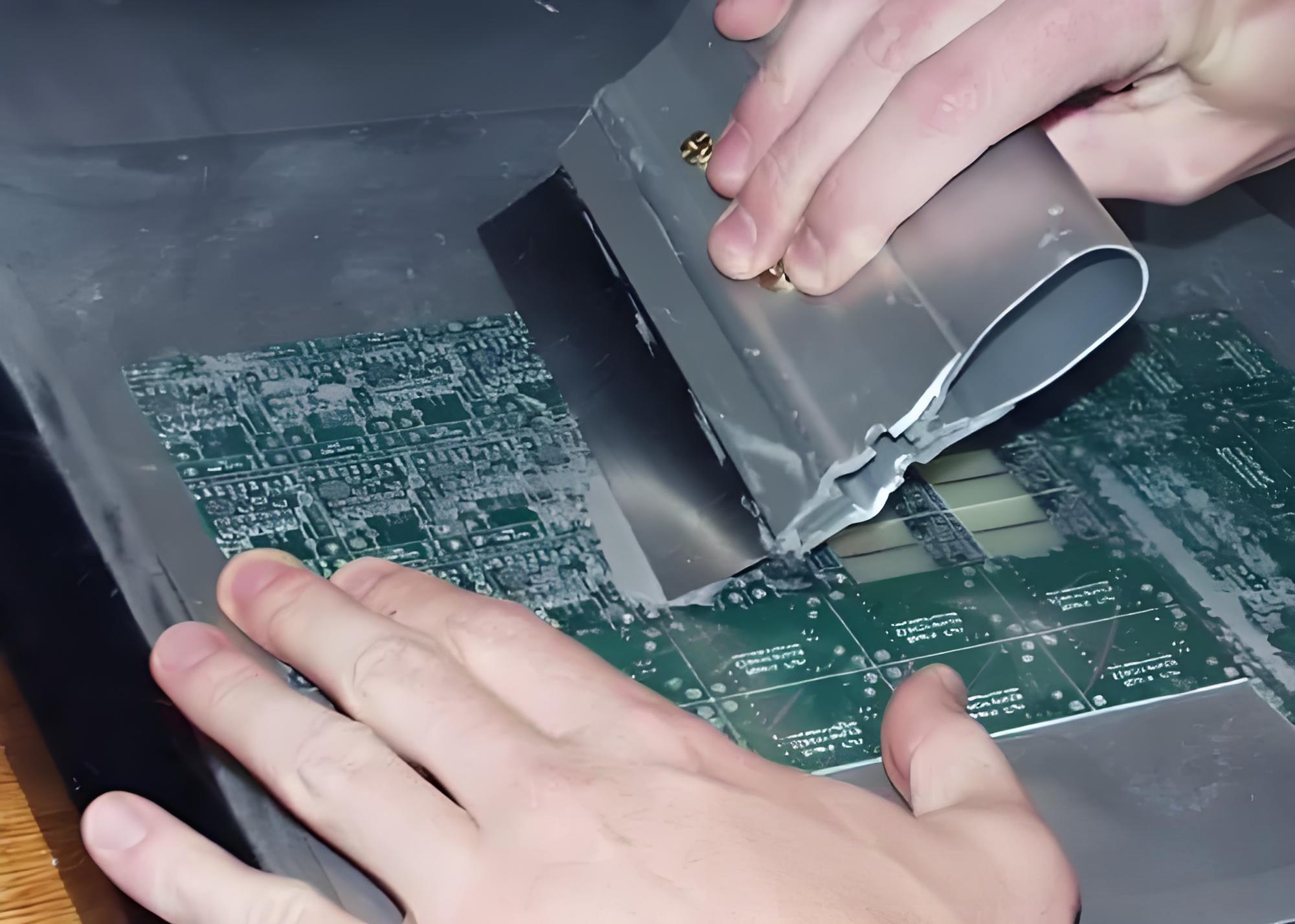
How to Make PCB Stencil?
Below are how to make PCB stencil:
- Material Selection: First, choose the appropriate stencil material based on the requirements of the PCB assembly, such as the type of components, production volume, and environmental conditions. As mentioned earlier, options include stainless steel, nickel – plated steel, aluminum, polymer – based materials, or titanium.
- Design Transfer: Transfer the approved stencil design, which includes the layout of apertures, frame details, etc., to the manufacturing equipment. This can be done through digital files, such as Gerber files, which are widely used in the PCB manufacturing industry.
- Laser – Cutting (for Laser – Cut Stencils): If a laser – cut stencil is being made, a high – power laser is used to precisely cut the apertures in the stencil material. The laser beam is controlled to follow the design pattern, creating clean and accurate cuts. The laser power and cutting speed are carefully adjusted based on the thickness and type of the stencil material.
- Electroforming (for Electroformed Stencils): In the electroforming process, a patterned mandrel is created first. This mandrel has the inverse shape of the desired stencil apertures. The mandrel is then placed in an electroplating bath, and metal ions are deposited onto the mandrel surface. Over time, a thick layer of metal builds up, forming the stencil. After the desired thickness is achieved, the mandrel is removed, leaving behind the electroformed stencil with smooth – walled apertures.
- Etching (for Etched Stencils): For etched stencils, the stencil material is first coated with a photoresist layer. The design is then transferred to the photoresist using a photomask and exposure to ultraviolet light. The unexposed areas of the photoresist are removed, and the stencil material is then etched using a chemical etchant. The etchant dissolves the exposed areas of the stencil material, creating the apertures.
- Composite Stencil Assembly (for Composite Stencils): If making a composite stencil, the different materials are assembled together. For example, a polymer coating may be applied to a metal stencil base using a suitable bonding method, such as adhesive bonding or thermal bonding.
- Multilevel Stencil Fabrication (for Multilevel Stencils): In the case of multilevel stencils, multiple layers of stencil material with different aperture levels are fabricated separately and then assembled together. This may involve precise alignment and bonding techniques to ensure the correct registration of the different levels.
- Quality Inspection: After the stencil is fabricated, it undergoes a thorough quality inspection. This includes checking the dimensions of the apertures, the flatness of the stencil surface, and the integrity of the frame. Any defects, such as mis – cut apertures, rough surfaces, or frame deformities, are identified and corrected.
- Marking and Packaging: Once the stencil passes the quality inspection, it is marked with relevant information, such as part numbers and manufacturing details. The stencil is then carefully packaged to prevent damage during transportation and storage.
How To Choose A Reliable SMT Stencil PCB Manufacturer?
Here are methods about how to choose a reliable SMT stencil PCB manufacturer:
- Experience and Reputation: Choose manufacturers with long – standing industry presence. A company with 10 – 20+ years of experience has likely handled diverse stencil requirements and refined manufacturing processes. Check online reviews, testimonials, and industry references for reputation.
- Quality Control Measures: Ask about the manufacturer’s quality control. Reliable ones have multiple inspection points, from material to final product checks, and can provide inspection reports as quality control documentation.
- Technology and Equipment: Manufacturers should use advanced tech like high – precision laser – cutting machines for laser – cut stencils or electroforming facilities. Modern equipment ensures stencil accuracy and quality.
- Customization Capability: For custom stencils, the manufacturer must meet specific needs. They should have experienced engineers to optimize stencil designs for PCB assembly.
- Delivery Time and Logistics: Evaluate the manufacturer’s ability to meet delivery deadlines. They should offer a realistic production schedule and keep you updated on potential delays. Also, inquire about shipping and delivery safety.
- Cost – Effectiveness: While cost matters, it’s not the only factor. Ensure competitive pricing, compare quotes, and consider overall value including quality and service.
- Material Sourcing: Reliable manufacturers source high – quality materials. Inquire about the origin and quality certifications of the metals or polymers used for stencils to guarantee durability and performance.
- Customer Support: Good customer support is crucial. Manufacturers should offer prompt responses to inquiries, provide technical assistance during the design process, and be available for post – sale support.
- Environmental Compliance: Check if the manufacturer adheres to environmental regulations. Environmentally – conscious practices ensure sustainable production and minimize the impact on the planet.
How Much Does A PCB Stencil Cost?
The cost of a PCB stencil can vary significantly, typically ranging from $50 to $1000+. A basic laser-cut stainless-steel stencil for small to medium-sized PCBs with standard apertures generally costs $50 – $200. In contrast, complex stencils with fine-pitch apertures, custom geometries, or multi-level designs can cost $200 – $1000 or more. Electroformed stencils, prized for their precision, usually fall on the higher end of this range.
Factors influencing PCB stencil prices:
- Complexity: Intricate designs with small apertures (e.g., fine-pitch components) require more precise manufacturing, increasing costs.
- Material: Premium materials like electroformed nickel or high-grade stainless steel are more expensive than standard options.
- Size: Larger stencils demand more material and longer processing times.
- Quantity: Ordering multiple stencils can reduce the per-unit cost due to economies of scale.
- Finish and Special Features: Additional treatments (e.g., Nano-coating) or custom features add to the price.
Strategies to reduce PCB stencil costs:
- Simplify Design: Prioritize standard aperture sizes and avoid unnecessary custom shapes.
- Material Selection: Choose cost-effective stainless steel grades suitable for your application instead of high-end materials.
- Bulk Orders: Purchase multiple stencils at once to leverage volume discounts.
- Negotiate with Suppliers: Establish long-term partnerships or negotiate prices based on order frequency.
- Design for Manufacturability (DFM): Work with manufacturers to optimize the design for efficient production.*
Conclusion
In conclusion, Stencil PCBs are an integral part of the SMT process, and understanding their various aspects, from materials and types to design and manufacturing, is essential for successful PCB assembly. When choosing a manufacturer, it’s crucial to consider factors like experience, quality control, and customization capabilities. The cost of PCB stencils can be managed through smart design choices and volume ordering. If you have any request for stencil PCB board, welcome to contact EBest Circuit (Best Technology).