EBest Circuit (Best Technology) Co.,Ltd
- +86-755-2909-1601
- sales@bestpcbs.com
What Multi-Layer SinkPAD Board is?
Multi-layer SinkPAD Board refer to metal core board have more than 2 layers of trace circuits, on the same side, or on both top and bottom side, and have direct thermal path (PAD). They are rarely used as normally the trace layout was not so complex that need more than 2 layers of trace circuit, but still available.
You can put more trace layers on one side and still keep good direct thermal path, like bellowing 4L SinkPAD board.

The 4 Layers SinkPAD board consists of four layers of trace circuit on same side, a dielectric (non-conducting) layer, a metal core/pedestal which normally is copper. As there’re four layers of trace circuits, so engineer can put more traces into the circuit on the same size circuit and then design more complicated board than 1 Layer SinkPAD board , or 2L SinkPAD board.
Or you separate trace layers on both top and bottom sides, so there’re two layers on each side, that are 4L Double Sided SinkPAD Board.
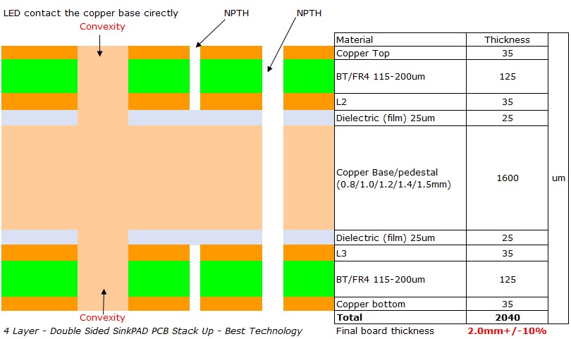
There’s also no PTH (plated through hole) on double sided SinkPAD board, because the limitation of manufacturing process, which different from Multi-layers Metal Core PCB which has a lot of PTH, and thermal PAD of LED will be put directly on copper core, also belonging to Direct Thermal Path (DTP) board too, but engineer needs to consider where the heat sink will be if he want more fast heat transferring, as there’re always components on both sides, and that make double sides multi-layers SinkPAD board designing becoming more difficult & complex comparing to 1L SinkPAD board , or 2L SinkPAD board.
Advantages of Utilizing Multi-Layer SinkPAD Board:
Application of Multi Layers SinkPAD Board
Multi Layers SinkaPAD Board Capability |
|
Click here to see the manufacturing process of Multi layers SinkPAD Board and other options.
If you want to customize Multi-layer of SinkPAD board, please contact EBest Circuit (Best Technology) and send your request for SinkPAD Board(SinkPAD PCB) today.
ISimply drop your email or phone number in the contact form, and we'll promptly provide you with a quotation.