





High-power electronics often require efficient heat dissipation and dense circuit routing within limited PCB space. A Blind and Buried Vias SinkPAD PCB combines multilayer electrical connections with a direct thermal path, but the via structure and copper pedestal must be carefully integrated to avoid manufacturing and reliability problems.
EBest Circuit provides custom copper-core SinkPAD PCB manufacturing, free DFM review, engineering support, and PCB assembly services. For projects requiring blind and buried vias, our engineers can evaluate the layer connections, copper pedestal geometry, and manufacturing options to help you move from prototype to production.
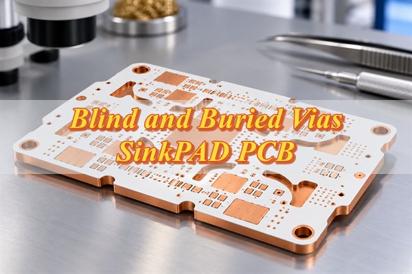
Can Blind and Buried Vias Be Integrated Into SinkPAD PCB?
Blind and buried vias can be considered for multilayer SinkPAD PCB designs when the electrical connections can be formed without interfering with the copper core or direct thermal path. Their feasibility depends on the circuit layer arrangement and manufacturing process.
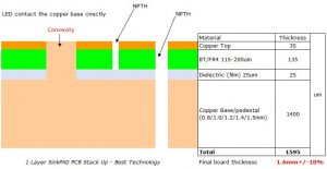
Blind vias connect an outer circuit layer to an internal layer, while buried vias connect internal layers without reaching the finished board surfaces. A SinkPAD PCB uses a raised copper pedestal to transfer heat directly from a compatible component thermal pad into the copper substrate.
The main structural considerations include:
- Circuit Layer Arrangement: Blind and buried vias are generally easier to accommodate when the required electrical layers are positioned on the same side of the copper core.
- Electrical Isolation: Plated vias must remain separated from the copper substrate unless an electrical connection is intentionally required.
- Copper Pedestal Geometry: The thermal contact area must remain accessible and properly aligned with the component’s thermal pad.
- Via Processing: Internal connections may require drilling, plating, and lamination before the circuit structure is integrated with the copper base.
Double-sided SinkPAD PCB presents additional challenges because the metal core separates the circuit layers on opposite sides. Conventional plated through-holes cannot simply pass through the copper substrate as they would in a standard multilayer FR4 PCB.
For complex layouts, keeping the electrical interconnections within a manufacturable circuit stack helps preserve the direct thermal path.
Which SinkPAD PCB Stackups Are Suitable for Blind and Buried Vias?
A same-side multilayer SinkPAD PCB offers a practical starting point for designs requiring complex interlayer connections. It provides additional routing space without requiring vias to pass through the copper substrate.
| SinkPAD PCB Structure | Circuit Configuration | Via Design Considerations |
|---|---|---|
| Single-Layer SinkPAD PCB | One circuit layer above the copper base | Blind and buried vias are unnecessary |
| 2-Layer SinkPAD PCB | Two circuit layers on one side of the copper core | Interlayer connections are possible; buried vias are generally unnecessary |
| 4-Layer Same-Side SinkPAD PCB | Four circuit layers above the copper base | Blind and buried via arrangements may be considered within the circuit stack |
| 4-Layer Double-Sided SinkPAD PCB | Two circuit layers on each side of the copper core | Conventional plated through-hole connections across the core are restricted |
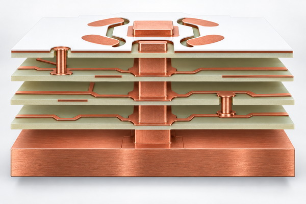
For example, a four-layer circuit stack positioned entirely above the copper base could use an L1–L2 blind via to connect a surface component to an internal trace. An L2–L3 buried via could provide another connection between inner circuit layers.
These connections require a compatible circuit construction and fabrication sequence. When the routing requirements can be met with fewer layers or simpler vias, a less complex stackup usually offers an easier manufacturing route.
When Do High-Power Electronics Need Blind and Buried Vias in SinkPAD PCB?
Blind and buried vias become useful when high-power components share limited board space with dense control, power distribution, or monitoring circuits. Heat generation alone does not justify using complex via structures.
- High-Power LED Lighting: Compact LED modules may combine multiple emitters, current regulation, and protection circuits. Additional circuit layers help accommodate routing while copper pedestals provide direct thermal contact beneath the LEDs.
- Automotive LED Headlights: Matrix lighting systems can contain many independently controlled LED channels. Blind and buried vias may help accommodate driver connections and monitoring circuits within a restricted board area.
- Industrial UV LED Equipment: High-intensity UV modules generate concentrated heat during continuous operation. Multilayer construction becomes useful when the equipment also requires complex power distribution and control connections.
- Compact Power Electronics: Some power semiconductor assemblies combine high-current devices with sensing and control circuits. A direct copper-core thermal path can be useful when the component’s thermal pad electrical potential is compatible with the substrate.
For simpler LED modules, a conventional two-layer SinkPAD PCB may provide adequate routing and thermal performance. More complex interconnections are worthwhile when board size or routing congestion makes them necessary.
What Are the Key Design Requirements for Blind and Buried Vias SinkPAD PCB?
The most important design requirements involve via layer connections, copper pedestal geometry, electrical isolation, and the thermal interface. These features determine whether the board can be manufactured and assembled reliably.
- Via Layer Span: Specify the starting and ending layers of each blind or buried via. The drill drawing should clearly identify internal connections and distinguish them from any proposed connection across the copper core.
- Via Diameter and Depth: Select hole dimensions according to the layer span and drilling method. Excessive aspect ratios or insufficient plating access can weaken electrical connections.
- Copper Pedestal Dimensions: Match the pedestal contact area to the component’s thermal pad. Height variation or poor alignment can reduce solder contact and affect heat transfer.
- Via-to-Pedestal Clearance: Maintain sufficient separation between electrical vias and the copper pedestal wherever contact is not intended. Operating voltage, dielectric properties, and manufacturing tolerances influence the required clearance.
- Dielectric Insulation: Choose suitable insulating materials and thicknesses to maintain electrical separation between circuit conductors and the copper substrate.
- Thermal Pad Electrical Potential: Confirm whether the component’s thermal pad is electrically neutral, grounded, or connected to an active terminal. Direct contact with a shared copper base must be compatible with the circuit.
- Via Filling and Pad Design: Vias located beneath solderable component pads may require filling, planarization, and copper capping to prevent solder wicking and maintain a flat mounting surface.
- Copper Thickness and Current Capacity: Match circuit copper thickness and trace widths to the electrical load. The copper substrate helps spread heat but does not replace adequate current capacity in electrically isolated traces.
- Heat Sink Interface: Consider how heat leaves the copper base. Thermal interface materials, mounting pressure, and external cooling conditions affect the final component temperature.
A complete stackup drawing, drill chart, and copper pedestal drawing make it easier to identify structural conflicts before prototype fabrication.
What Are the Main Manufacturing Challenges and Solutions for Blind and Buried Vias SinkPAD PCB?
The main manufacturing challenges involve precision via processing, copper pedestal alignment, electrical insulation, and multilayer stability. Poor control of these features can cause electrical defects, weak thermal contact, or premature connection failures.
- Via Drilling and Metallization Blind and buried vias require accurate drilling and consistent copper plating. Incorrect drill depth, layer misalignment, or insufficient metallization can produce open circuits or weak interlayer connections. Solution: Arrange the drilling and plating sequence according to the required via spans. Internal connections can be formed while their circuit layers remain accessible, with critical features verified through electrical testing and microsection inspection.
- Copper Pedestal Alignment The copper pedestal must match the position and dimensions of the component’s thermal pad. Misalignment or height variation can reduce the contact area and affect solder joint formation. Solution: Control pedestal geometry during copper-core processing and inspect critical dimensions against the approved component footprint.
- Electrical Isolation Around the Copper Core Plated vias and circuit traces may sit close to the conductive copper substrate. Inadequate insulation or registration errors can cause unintended electrical connections. Solution: Maintain appropriate dielectric separation and clearance around conductive features. Electrical continuity and insulation testing help detect manufacturing defects.
- Multilayer Lamination and Warpage Copper and dielectric materials expand differently during thermal processing. Excessive stress can affect layer alignment, internal connections, and board flatness. Solution: Select compatible materials, control lamination conditions, and inspect critical interfaces for displacement, separation, or distortion.
- Internal Via Reliability Repeated temperature changes place mechanical stress on plated connections. Stacked microvias are especially sensitive to defects at their internal copper interfaces. Solution: Use simpler or staggered via arrangements where possible. For stacked structures, suitable filling, plating control, and reliability verification help reduce connection failure risks.
Addressing these problems during the engineering review helps reduce prototype revisions and improves the consistency of subsequent production.
How Is a SinkPAD PCB With Blind and Buried Vias Manufactured?
Manufacturing a SinkPAD PCB with blind and buried vias requires coordinated circuit fabrication, via processing, copper pedestal formation, and lamination. The fabrication sequence is determined by the approved stackup and layer connections.
The main manufacturing stages are:
- Engineering Review and Stackup Preparation Review Gerber files, drill data, circuit layer positions, dielectric materials, and copper pedestal drawings. Establish the electrical connections and direct thermal contact areas.
- Inner-Layer Circuit Fabrication Produce the required internal circuit patterns on the specified materials. Prepare the circuit subassembly according to the approved layer arrangement.
- Blind and Buried Via Processing Form the required internal connections while the target layers are accessible. Buried vias are completed before the relevant inner layers are enclosed by later lamination. Blind vias are processed according to their layer span and selected build-up sequence.
- Copper Pedestal Formation Process the copper substrate to create the raised thermal contact areas. Control pedestal height, position, and dimensions to match the component footprints.
- Lamination and Circuit Integration Align and bond the circuit structure with the copper substrate using compatible insulating materials. Maintain electrical isolation while leaving the specified thermal contact areas exposed.
- Surface Finishing and Final Inspection Apply solder mask and the specified surface finish, complete board profiling, and inspect the finished dimensions. Electrical tests and relevant structural inspections verify the fabricated board.
Complex blind and buried via arrangements may require additional drilling, plating, or sequential lamination before the final copper-core integration.
How Are SinkPAD PCBs With Blind and Buried Vias Tested for Reliability?
Reliability testing checks the electrical connections, dielectric insulation, copper pedestal geometry, and thermal performance. Both electrical and thermal verification are important because a board can pass continuity testing while still having inadequate thermal contact.
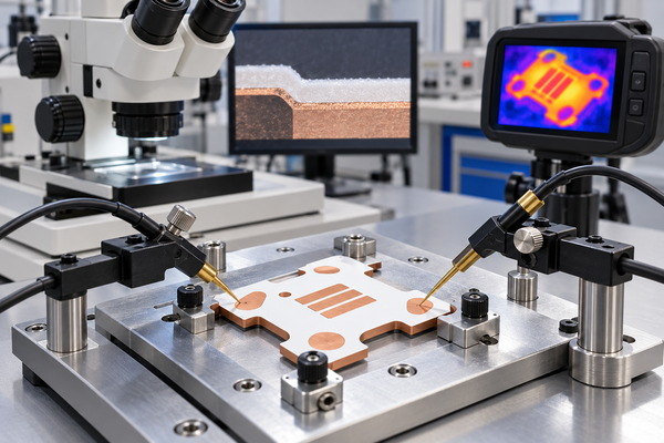
- Via Continuity Testing: Detects open circuits and verifies the intended blind and buried via connections.
- Electrical Insulation Testing: Checks separation between unrelated conductors and the copper substrate.
- Microsection Inspection: Examines internal vias, copper plating, layer connections, and dielectric interfaces for structural defects.
- Copper Pedestal Inspection: Measures pedestal height, position, and contact dimensions.
- Assembly Inspection: Evaluates solder joints and component placement. X-ray inspection can help assess hidden joints beneath suitable component packages.
- Thermal Performance Testing: Measures component or board temperatures under defined power, ambient temperature, and cooling conditions.
- Thermal Cycling: Evaluates the stability of critical interconnections and material interfaces under repeated temperature changes.
The thermal result depends on the complete assembly, including the component package, solder interface, copper pedestal, substrate, and external heat sink. Application-specific tests and acceptance criteria can be arranged according to the product’s operating requirements.
What Affects the Lead Time of Custom Blind and Buried Vias SinkPAD PCB?
Lead time depends on the layer structure, via processing requirements, copper pedestal complexity, and inspection scope. Additional drilling or lamination operations can extend manufacturing compared with conventional SinkPAD PCB production.
The main factors include:
- Circuit Layer Count: More layers can increase circuit fabrication and alignment work.
- Blind and Buried Via Structure: Multiple via spans may require additional drilling, plating, and sequential lamination.
- Copper Pedestal Complexity: Intricate geometries and tight dimensional tolerances can increase processing and inspection time.
- Material Availability: Copper base thickness, dielectric construction, and surface finishes affect manufacturing preparation.
- Prototype Qualification: New structures may require additional microsection inspection, thermal evaluation, or manufacturing adjustments.
- Production Quantity: Panel utilization, batch scheduling, and inspection requirements influence delivery planning.
For conventional multilayer SinkPAD PCB, EBest Circuit’s reference lead time is approximately 3–4 weeks for prototypes and 4–6 weeks for volume production. Special blind and buried via combinations require a schedule based on the actual manufacturing process.
Why Choose EBest Circuit for Custom SinkPAD PCB Manufacturing?
EBest Circuit helps you reduce manufacturing risks, improve PCB reliability, and simplify production with engineering support and customized SinkPAD PCB services.
- Custom SinkPAD PCB Solutions: Get copper-core SinkPAD PCBs tailored to your thermal, electrical, and structural requirements.
- Free DFM Review: Identify potential via, copper pedestal, and insulation issues early to reduce costly design revisions.
- Engineering Support: Get practical solutions for complex stackups, thermal management, and manufacturing challenges.
- Quality Assurance: Use controlled manufacturing, applicable ISO, IATF 16949, and AS9100D quality-system documentation, and project-specific inspection support. Confirm the applicable manufacturing site and certificate scope during supplier qualification.
- One-Stop PCB and PCBA Services: Save time with PCB fabrication, component sourcing, SMT/THT assembly, and testing services.
- Prototype to Mass Production: Validate your design with prototypes and receive manufacturing support for repeat production.
FAQs About Blind and Buried Vias SinkPAD PCB
Q1: Can an existing MCPCB design be converted into a SinkPAD PCB?
A1: In some cases, the original circuit layout can be reused. However, the copper pedestal, dielectric openings, and thermal pad arrangement may need modifications to create the direct thermal path.
Q2: Does a copper-core SinkPAD PCB still need an external heat sink?
A2: Often, yes. The copper base spreads and transfers heat, but the assembly still needs a suitable cooling path. External heat sink requirements depend on component power, operating conditions, and mechanical construction.
Q3: Can multiple LEDs share the same copper pedestal?
A3: This may be possible when their thermal pad electrical potentials are compatible and the contact area supports the thermal requirements. Component spacing and soldering conditions must also be considered.
Q4: Do thick copper SinkPAD boards require different SMT reflow profiles?
A4: Their higher thermal mass can affect heating and cooling during reflow. The soldering profile should account for board construction, solder paste, component temperature limits, and measured temperatures.
Q5: Which surface finishes are suitable for SinkPAD PCB assembly?
A5: ENIG, ENEPIG, Immersion Tin, and OSP are available for applicable SinkPAD constructions. The choice depends on soldering requirements, component attachment methods, and storage conditions.
Q6: Can mounting holes be placed close to copper pedestals?
A6: Yes, provided adequate mechanical clearance and electrical isolation are maintained. Mounting forces should not deform the thermal contact area or damage nearby circuit features.
Q7: Can components on a SinkPAD PCB be repaired or replaced?
A7: Rework is possible for suitable assemblies, although the copper base absorbs substantial heat during soldering. Controlled preheating and temperature monitoring help reduce the risk of damage to components and surrounding joints.
Q8: How should SinkPAD PCBs be stored before assembly?
A8: Boards should be protected from moisture, contamination, and mechanical damage. Packaging conditions and shelf life depend on the selected surface finish and assembly requirements.
How Can You Get a Custom SinkPAD PCB Quote and Free DFM Review?
For a Blind and Buried Vias SinkPAD PCB quote, EBest Circuit offers custom fabrication, free DFM review, engineering support, prototyping, and PCB assembly services for high-power electronics. Send your Gerber files, stackup drawing, via specifications, copper pedestal dimensions, thermal requirements, order quantity, required delivery date, and delivery location to sales@bestpcbs.com. Our engineering team can review your design, recommend suitable manufacturing options, and provide a quotation based on your project requirements.
You may also like

Tags: Blind and Buried Vias PCB, High-Power Electronics PCB, multilayer sinkpad pcb, sinkpad pcb