





A LoRa sensor can work perfectly on a test bench but lose communication range once its battery and enclosure are installed. The problem often lies in the antenna, not the radio module. A LoRa PCB antenna depends on its operating frequency, ground plane, physical dimensions, and RF matching network. Even a small layout change can shift its resonant frequency or reduce radiation efficiency.
This guide explains how to design a LoRa PCB antenna for 433, 470, 868, and 915 MHz IoT devices, covering antenna selection, initial dimension calculations, PCB layout, impedance matching, simulation, prototype tuning, and manufacturing requirements.
What Should You Consider Before Designing a LoRa PCB Antenna?
Start with the operating frequency, available PCB space, RF interface, and target antenna performance. These requirements determine which LoRa PCB antenna structure is practical and whether the available board area can support the intended communication range.
| Parameter | Design Requirement |
|---|---|
| Operating frequency | 433, 470, 868, or 915 MHz |
| Frequency coverage | Required channels and operating bandwidth |
| RF interface | Typically a nominal 50Ω antenna port |
| Antenna space | Available PCB area and board‑edge clearance |
| PCB stackup | Material, dielectric thickness, and copper layers |
| Ground plane | Dimensions and geometry required by the antenna |
| Enclosure | Battery, housing, shielding, and nearby metal |
| RF performance | S11, VSWR, radiation efficiency, and gain |
Define the entire operating band rather than only the center frequency. For example, a North American LoRaWAN device may use channels within 902–928 MHz. An antenna matched at 915 MHz alone may not perform adequately across every required channel.
Regional frequency regulations must also be checked. The availability and permitted operating conditions of 433, 470, 868, and 915 MHz vary between countries. The selected frequency band should be confirmed before antenna dimensions and layout are finalized.
Which Antenna Type Is Best for Your LoRa PCB Design?
A printed monopole is a practical starting point when PCB space is available, while an inverted‑F antenna (IFA) is worth considering for compact layouts with controlled feed and ground geometry. If space is particularly limited, a meandered structure can reduce the footprint, although bandwidth and radiation efficiency must be verified.
| Antenna Structure | Space Requirement | Design Considerations | Recommended Use |
|---|---|---|---|
| Printed Monopole | Requires sufficient space for the radiating element and ground structure | Simple geometry; efficiency and bandwidth depend on electrical size and ground dimensions | LoRa devices with adequate PCB space |
| Inverted‑F Antenna (IFA) | Can use a compact, folded radiating structure | Feed and shorting positions affect impedance; ground geometry must be controlled | Compact IoT devices requiring adjustable antenna impedance |
| Meandered Monopole / MIFA | Reduces the physical footprint through folded traces | Trace coupling increases tuning sensitivity and may reduce bandwidth and efficiency | Space‑constrained sensors and compact LoRa modules |
A meandered antenna is a miniaturized implementation of a monopole or inverted‑F structure, not a completely separate antenna operating principle. Its performance depends on the conductor path, spacing between folded sections, and PCB ground plane.
For 433 MHz and 470 MHz, the longer wavelength makes compact printed antennas more challenging. A folded or loaded structure may be necessary, but excessive miniaturization can reduce efficiency and usable bandwidth. At 868 MHz and 915 MHz, shorter wavelengths make printed monopole and inverted‑F structures easier to integrate into compact IoT products.
Choose the antenna according to available PCB area, ground‑plane dimensions, operating bandwidth, and radiation efficiency requirements. Start with a proven reference design for the intended frequency, then validate its performance using the actual PCB geometry and enclosure.
How Do You Connect a LoRa Module to a PCB Antenna?
For a LoRa module with a 50Ω RF antenna port, connect the module to the printed PCB antenna through a controlled‑impedance RF feed and any required antenna matching network. If the module already includes an integrated antenna, follow its placement and clearance requirements instead of adding another antenna connection.
The connection method depends on the module’s RF interface.
| Connection Method | RF Connection | Design Requirements |
|---|---|---|
| Integrated module antenna | Antenna printed directly on the module | Follow the manufacturer’s placement, ground, and copper‑clearance requirements |
| Host PCB antenna | Module ANT port → PCB RF feed → antenna matching → printed antenna | Confirm RF port impedance, feed structure, and antenna ground geometry |
| IPEX/U.FL PCB antenna | Module RF port → RF connector → coaxial cable → separate PCB antenna | Verify connector compatibility, cable impedance, routing, and antenna mounting position |
| SMA antenna interface | Module RF port → PCB feed → SMA connector → external antenna | Control connector launch geometry, grounding, and mechanical attachment |
Before routing the RF connection, check the following:
- RF port impedance: Confirm whether the module provides a nominal 50Ω antenna interface or requires external RF matching and filtering.
- Frequency compatibility: Verify that the module and selected antenna support the same operating band.
- RF feed structure: Use a controlled‑impedance trace with a suitable reference ground along the feed section.
- Antenna clearance: Preserve the ground and copper keep‑out requirements specified for the chosen antenna.
- Matching provision: Reserve tuning components where recommended by the module or antenna reference design.
A bare LoRa transceiver IC is different from a complete RF module. Its RF pins may require a manufacturer‑specified matching, filtering, or balanced‑to‑unbalanced conversion circuit before connecting to a 50Ω antenna feed. Do not assume that every transceiver output can connect directly to a printed antenna.
For an integrated PCB antenna, preserve the intended RF interface and ground geometry through prototype verification. If the antenna connection, PCB layout, or enclosure changes, recheck the antenna impedance before production.
How Do You Estimate Antenna Dimensions for 433/470/868/915 MHz?
The initial length of a LoRa PCB antenna can be estimated using the quarter‑wavelength formula:
L = c / (4 × f)
Where:
- L: Quarter‑wavelength in meters (m).
- c: Speed of light, approximately 300,000,000 m/s.
- f: Operating frequency in hertz (Hz).
For calculations using MHz and millimeters, the formula becomes:
L (mm) = 75,000 / Frequency (MHz)
The following table shows the approximate free‑space wavelength and corresponding quarter‑wavelength for each frequency.
| Frequency | Wavelength (λ) | Quarter‑Wave Length (λ/4) |
|---|---|---|
| 433 MHz | 692.8 mm | 173.2 mm |
| 470 MHz | 638.3 mm | 159.6 mm |
| 868 MHz | 345.6 mm | 86.4 mm |
| 915 MHz | 327.9 mm | 82.0 mm |
These values are initial free‑space references, not finished PCB antenna dimensions. Actual dimensions depend on the antenna structure, dielectric loading, ground plane, and coupling between conductors.
For example, the calculated quarter‑wavelength at 915 MHz is approximately 82 mm. A meandered antenna may occupy a much smaller PCB footprint, but folding the conductive path changes its electromagnetic behavior. Simply fitting 82 mm of copper trace into a compact shape does not guarantee resonance at 915 MHz.
The design implications differ by frequency:
- 433 MHz: The long wavelength makes compact PCB antennas difficult to implement without significant miniaturization.
- 470 MHz: Slightly shorter dimensions than 433 MHz, although ground‑plane size and antenna efficiency remain major constraints.
- 868 MHz: More manageable electrical dimensions for compact monopole and inverted‑F structures.
- 915 MHz: Similar antenna structures to 868 MHz, but the matching and bandwidth must cover the required operating channels.
Use the calculated length to establish an initial geometry. Final antenna dimensions must be verified through electromagnetic simulation and prototype tuning, especially when using meandered traces or electrically small antenna structures.
How Do PCB Materials and Stackups Affect Antenna Design?
FR-4 is suitable for many Sub‑GHz LoRa PCB antenna applications, but its dielectric properties and the PCB stackup affect resonance, impedance, and radiation efficiency. Material selection should follow the electrical requirements rather than assuming that every RF antenna requires a specialized high‑frequency laminate.
The main parameters are:
- Dielectric constant (Dk): Influences effective wavelength and the antenna’s resonant behavior.
- Dissipation factor (Df): Contributes to dielectric loss, which can reduce radiation efficiency.
- PCB thickness: Changes the electromagnetic field distribution and interaction with nearby ground layers.
- Copper construction: Trace dimensions, copper thickness, and conductor losses affect impedance and antenna performance.
For simulation, use the selected material’s electrical properties at relevant frequencies rather than relying on a generic FR-4 dielectric constant.
A two‑layer PCB can support a printed LoRa antenna, while a four‑layer PCB may provide more flexibility for RF routing, power distribution, and digital circuit separation. However, additional copper layers can affect antenna performance if they extend into areas that must remain clear.
The radiating structure and RF feed may require different copper arrangements. The antenna must follow its specified ground and keep‑out geometry, while the feed requires a controlled impedance reference.
Keep the validated PCB material and stackup consistent between prototype and production. Changes in dielectric thickness, laminate properties, or nearby copper may shift the antenna’s resonant frequency and require retuning.
What Are the Key PCB Layout Rules for LoRa Antennas?
Position the antenna where its required ground plane and radiation clearance can be maintained. Poor placement can reduce antenna efficiency even when the trace dimensions and matching network are otherwise correct.
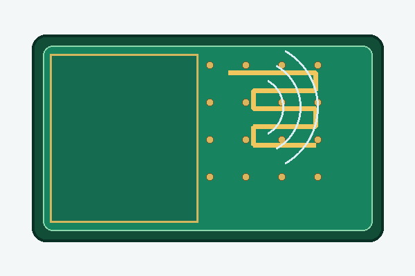
Follow these PCB layout rules:
- Antenna position: Place the radiating element near a suitable PCB edge or corner, following the selected reference design.
- Ground plane: Maintain the specified ground dimensions, continuity, and antenna‑to‑ground relationship.
- Copper keep‑out: Remove copper, signal traces, and vias from the required antenna clearance areas on all applicable layers.
- Component spacing: Keep batteries, metal shields, connectors, and other conductive parts away from the radiating region.
- Noise separation: Avoid placing switching regulators, clocks, and high‑speed digital traces close to the antenna.
- Enclosure clearance: Account for housing materials, nearby metal, mounting hardware, and final antenna orientation.
The antenna radiator and RF feed line have different grounding requirements. The feed normally requires a defined reference plane, while the radiating element follows antenna‑specific ground and clearance rules.
For a LoRa meander line PCB antenna, spacing between adjacent conductor sections is particularly important. Reducing this spacing can save PCB area but increases electromagnetic coupling, potentially changing resonance, bandwidth, and efficiency.
The final layout should also account for mechanical integration. A printed antenna that performs well on an uncovered PCB can behave differently after a battery, display, or enclosure is installed nearby.
How Do You Design the RF Feed Line and Matching Network?
Design the RF feed for the required interface impedance, typically 50Ω, and use the antenna matching network to transform the antenna’s measured input impedance. Antenna matching should be distinguished from the transceiver’s RF output matching and harmonic filtering.
A typical RF connection follows this path:
RF Front End → 50Ω Feed Line → Antenna Matching Network → PCB Antenna
For a module with a specified 50Ω antenna port, the transceiver‑side matching and filtering may already be integrated. A bare transceiver IC may require additional RF circuitry according to its manufacturer’s reference design.
Focus on these requirements:
- Feed geometry: Calculate microstrip or grounded coplanar waveguide dimensions using the actual PCB stackup.
- Impedance continuity: Avoid unnecessary changes in trace width, reference ground, and routing geometry.
- Matching position: Place antenna matching components close to the feed point with short interconnections.
- Ground vias: Provide low‑inductance ground connections for shunt matching components.
- Component flexibility: Reserve suitable footprints for tuning without major PCB layout changes.
A π-type matching network is commonly used because its component positions support different impedance transformations. However, an L‑type network or another topology may be more suitable depending on the measured impedance and required bandwidth.
Do not copy matching component values from an unrelated PCB design. Antenna geometry, ground‑plane dimensions, feed parasitics, and nearby mechanical components can change the impedance significantly.
For multi‑band applications, verify that the matching network provides acceptable performance throughout the required frequency ranges rather than only at one center frequency.
How Do You Simulate a LoRa PCB Antenna Before Prototyping?
Electromagnetic simulation helps determine whether an antenna geometry can meet its RF requirements before fabrication. It is particularly useful for compact Sub‑GHz antennas, where folded traces, ground‑plane dimensions, and nearby components influence resonance and radiation efficiency.
Full‑wave simulation tools such as Ansys HFSS and CST Studio Suite can evaluate the antenna’s electromagnetic characteristics.
A practical simulation process includes five steps.
Step 1: Build the antenna geometry.
Create the selected monopole, inverted‑F, or meandered structure using the initial dimensions. Include trace width, spacing, feed point, and shorting connections where applicable.
Step 2: Apply the PCB construction.
Define the laminate’s dielectric properties, PCB thickness, copper layers, ground geometry, and antenna clearance areas.
Step 3: Configure the frequency sweep.
Cover the intended operating band and include enough additional frequency range to identify nearby resonances.
Step 4: Evaluate the results.
Check input impedance, S11, operating bandwidth, radiation efficiency, and radiation patterns.
Step 5: Optimize the geometry.
Adjust antenna dimensions, feed position, trace spacing, or ground geometry. Repeat the simulation until the design approaches its required performance targets.
| Parameter | Simulation Check |
|---|---|
| Resonant frequency | Position of resonance relative to the operating band |
| S11 | Input matching across the required frequencies |
| Input impedance | Resistance and reactance at the antenna feed |
| Bandwidth | Frequency range meeting the matching requirement |
| Radiation efficiency | Proportion of accepted RF power that is radiated |
| Radiation pattern | Directional radiation characteristics and polarization |
Do not optimize only for the lowest S11 value. A compact antenna can exhibit good impedance matching while losing a substantial portion of accepted power through conductor or dielectric losses.
Once the initial antenna geometry meets its targets, include nearby batteries, enclosure materials, and metal components where relevant. This helps identify detuning risks before manufacturing the first prototype.
How Do You Test and Tune a LoRa PCB Antenna?
Use a vector network analyzer (VNA) to measure S11 and complex input impedance. These measurements help identify the antenna’s resonant behavior and determine whether the matching network requires adjustment.
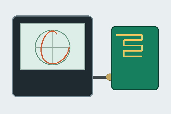
For a nominal 50Ω interface, S11 of -10 dB or lower is a common initial matching target, although the final acceptance requirement depends on the application.
| S11 (dB) | Reflected Power | VSWR |
|---|---|---|
| -6 dB | 25.1% | 3.01:1 |
| -10 dB | 10.0% | 1.92:1 |
| -15 dB | 3.2% | 1.43:1 |
| -20 dB | 1.0% | 1.22:1 |
These figures indicate impedance matching at the measurement reference plane. They do not represent antenna radiation efficiency or gain.
A practical tuning process follows five steps.
Step 1: Calibrate the VNA.
Establish the correct measurement reference plane and account for cables, connectors, and fixtures. Minimize unintended coupling from the RF test cable.
Step 2: Measure antenna impedance.
Record S11 and inspect the Smith chart to determine the resistive and reactive characteristics across the operating band.
Step 3: Adjust the matching network.
Select suitable component values according to the measured impedance. Repeat the measurement after each meaningful adjustment.
Step 4: Correct the antenna geometry if necessary.
If resonance or bandwidth remains unsuitable, review the antenna dimensions and ground structure instead of relying exclusively on matching components.
Step 5: Verify the complete operating band.
Measure across all required channels, including band edges, and record the final matching component values.
Common measurement problems can be diagnosed using the following table.
| Symptom | Possible Cause | First Check |
|---|---|---|
| Resonance below target | Excessive electrical length or additional loading | Radiator geometry and nearby conductors |
| Resonance above target | Insufficient electrical length or changed loading | Antenna dimensions and ground structure |
| Poor S11 | Impedance mismatch | Matching network and feed connection |
| Narrow bandwidth | High‑Q resonance or excessive miniaturization | Antenna structure and available space |
| Unstable measurements | Cable coupling or fixture effects | Calibration and cable isolation |
These resonance‑shift relationships are useful initial diagnostic clues, not universal rules for every antenna topology.
Final tuning should use the intended PCB construction and mechanical configuration. A matching network optimized on a bare PCB may require adjustment after the battery and enclosure are installed.
How Do You Verify LoRa PCB Antenna Performance in a Real Device?
Verify antenna performance with the final PCB assembly, battery, and enclosure installed. Nearby metal, dielectric materials, and mechanical components can alter resonance and radiation characteristics, even when the bare‑board antenna has acceptable impedance matching.
The main verification parameters are:
- Radiation efficiency: Measures the proportion of accepted RF power converted into radiated energy.
- Antenna gain: Describes radiation strength in a particular direction relative to a reference.
- Radiation pattern: Shows how radiated energy varies with direction.
- Polarization: Influences coupling between transmitting and receiving antennas.
- Communication performance: Confirms wireless link behavior under defined operating conditions.
Radiation efficiency, gain, and patterns require suitable over‑the‑air measurement methods, such as an anechoic chamber or another controlled antenna test environment. A VNA measurement of S11 alone cannot establish these characteristics.
For communication tests, keep transmit power, spreading factor, bandwidth, coding rate, antenna orientation, and environmental conditions consistent when comparing antenna configurations.
For example, a LoRa sensor may show acceptable matching before assembly but experience reduced received signal strength after a battery is positioned close to the radiator. In this case, evaluate the assembled device and determine whether antenna geometry, placement, or matching requires adjustment.
Communication range also depends on the complete RF link budget, including transmit power, receiver sensitivity, propagation loss, interference, and antenna orientation. A successful short‑distance packet test does not establish the maximum reliable communication range.
Record the approved antenna dimensions, matching component values, enclosure configuration, and verification results before releasing the design for production.
What Should Be Checked Before LoRa PCB Antenna Manufacturing?
PCB manufacturing must reproduce the antenna geometry and board construction validated during development. Changes in trace width, material thickness, copper clearance, or matching components can shift the antenna’s response.
Before fabrication and assembly, check:
- Antenna dimensions: Verify conductor width, spacing, geometry, and specified etching tolerances.
- PCB stackup: Confirm laminate, dielectric thickness, copper thickness, and layer construction.
- Copper clearance: Preserve antenna keep‑out areas on every applicable layer.
- Solder mask and surface finish: Maintain the coating and finish conditions used in the validated design.
- Matching components: Verify footprints, component values, placement, and ground connections against the approved BOM.
- Inspection requirements: Define PCB electrical tests, assembly inspection, and any project‑specific RF verification.
Prepare the Gerber files, drill files, stackup requirements, BOM, Pick‑and‑Place data, assembly drawings, and RF test specifications before requesting PCB manufacturing.
For production consistency, avoid unapproved changes to the antenna structure, substrate, matching components, or mechanical placement. Any necessary modification should be reviewed for its RF impact before release.
EBest Circuit supports LoRa PCB antenna projects with custom PCB fabrication, SMT assembly, and DFM technical guidance. Every EBest PCBA project is supported by a 1+3 technical team covering PE, DFM, Process, and Quality, helping customers review manufacturing requirements and maintain production consistency. Antenna and RF circuit design remain the customer’s responsibility.
FAQs About LoRa PCB Antenna Design
Q1: Does LoRa modulation require a special antenna?
A1: No. LoRa uses conventional RF antenna principles. The antenna must support the required frequency, impedance, bandwidth, and radiation characteristics. An antenna designed for another modulation method may also work with LoRa if its RF specifications are compatible.
Q2: Can one PCB antenna support both 868 MHz and 915 MHz?
A2: Yes, provided its matched bandwidth and radiation performance cover both required operating ranges. An antenna tuned only at 868 MHz cannot automatically be assumed to perform adequately at 915 MHz.
Q3: Does higher antenna gain always increase LoRa communication range?
A3: No. Higher gain usually concentrates radiation in certain directions. For mobile or randomly oriented IoT devices, a broader radiation pattern may be preferable. Gain, polarization, antenna orientation, and link budget all influence actual communication range.
Q4: Can flexible PCB materials be used for LoRa antennas?
A4: Yes. Flexible PCB antennas can fit curved or restricted spaces. However, substrate properties, bending conditions, and mounting geometry must remain consistent because changes can affect impedance and radiation performance.
Q5: Does increasing copper thickness improve antenna efficiency?
A5: Not necessarily. Thicker copper may reduce conductor resistance, but efficiency also depends on antenna geometry, dielectric losses, and radiation characteristics. Copper thickness alone does not determine antenna efficiency.
Q6: Can two LoRa radios share one antenna?
A6: Yes, with a suitable RF switching or combining network. The circuit must provide sufficient isolation, impedance matching, and transmitter protection. Two RF outputs should not be connected directly without an appropriate RF design.
Q7: Can a LoRa PCB antenna operate inside a metal enclosure?
A7: Metal can detune or shield the antenna. An external antenna, nonmetallic opening, or alternative mounting arrangement may be necessary. Verify antenna performance in the actual enclosure configuration.
Q8: Can the same LoRa antenna transmit and receive signals?
A8: Yes. Passive antennas are generally reciprocal, allowing the same structure to support transmission and reception at the same frequency. The RF circuit must provide suitable switching, filtering, and matching.
Q9: Does solder mask affect LoRa PCB antenna performance?
A9: It can. Solder mask changes the dielectric environment around the antenna conductor and may shift resonance. Use the coating arrangement validated during simulation and prototype testing rather than changing it without RF verification.
Q10: Does a certified LoRa module eliminate final‑product certification requirements?
A10: No. Module certification may simplify part of the approval process, but antenna changes, enclosure integration, and operating conditions can affect compliance. Check the module’s integration requirements and applicable regulations.
Q11: Can conformal coating be applied over a LoRa PCB antenna?
A11: It may be possible, but the coating introduces additional dielectric loading and can change antenna resonance. Verify the coated assembly before introducing conformal coating into production.
Q12: Does antenna orientation affect LoRa communication?
A12: Yes. Antenna orientation affects polarization alignment and the radiation pattern relative to the receiving antenna. Polarization mismatch and unfavorable positioning can reduce received signal strength even when impedance matching is acceptable.
Conclusion
A reliable LoRa PCB antenna starts with the correct operating frequency, antenna structure, and initial dimensions. Ground‑plane geometry, RF matching, and enclosure integration must then be evaluated together. For 433, 470, 868, and 915 MHz IoT devices, electromagnetic simulation, VNA tuning, and assembled‑device RF testing provide the verification required before moving into production.
Ready to manufacture your LoRa PCB antenna design? EBest Circuit provides custom PCB prototyping, fabrication, SMT assembly, and DFM technical support for RF applications. Send your Gerber files, BOM, PCB stackup, and production requirements to sales@bestpcbs.com for a manufacturing review and quotation.
You may also like


Tags: 433 MHz PCB Antenna, 868 MHz LoRa Antenna, 915 MHz LoRa Antenna, LoRa PCB Antenna, Sub-GHz Antenna Design