





Isola IS415 is a 200°C Tg, CAF-resistant epoxy laminate and prepreg system for reliable lead-free multilayer PCBs. It provides strong thermal endurance, stable dielectric behavior, broad construction options, and familiar FR-4 processing. Specify it only after confirming the stackup, material supply, impedance requirements, fabrication controls, and qualification plan.

What Is Isola IS415 PCB Material?
IS415 is a high-reliability epoxy laminate and prepreg system for multilayer printed wiring boards. Isola manufactures it with electrical-grade E-glass reinforcement and a multifunctional resin system. The supplied datasheet identifies a typical glass transition temperature of 200°C, decomposition temperature of 370°C, Dk of 3.72 at 2 GHz, and Df of 0.0120 at 2 GHz.
The product name can refer to both copper-clad laminate used as cores and uncured prepreg used to bond layers. It is therefore more accurate to specify the complete construction, including the material family, core and prepreg build, glass styles, copper type, finished thickness, and controlled-impedance requirements, than to place only a trade name on a drawing.
This material belongs to the high-Tg FR-4 process family, not the PTFE or ceramic-filled microwave family. It offers better thermal reliability than many conventional FR-4 systems while retaining familiar multilayer fabrication methods. Use it when thermal cycling, lead-free assembly, and predictable electrical behavior matter but a different fabrication platform is unnecessary.
Why Is IS415 Suitable for High-Reliability Multilayer PCBs?
The resin system supports high-reliability multilayers by combining thermal endurance, low expansion, CAF resistance, and production-friendly processing. Those features reduce several common failure risks, but reliability still depends on the finished stackup, hole geometry, lamination quality, plating, assembly profile, and acceptance testing.
- High thermal margin: A 200°C Tg, 370°C Td, T260 of 60 minutes, and T288 above 20 minutes help the resin system withstand lead-free processing and thermal excursions.
- Controlled Z-axis expansion: The datasheet lists 45 ppm/°C below Tg, 240 ppm/°C above Tg, and 2.8% total expansion from 50°C to 260°C. Lower total expansion helps limit stress on plated through-hole copper.
- CAF resistance: The resin system is identified as CAF resistant, supporting designs where closely spaced conductors must retain insulation integrity under electrical bias and moisture exposure.
- Stable electrical characteristics: Typical Dk remains close to 3.71–3.72 from 1 to 10 GHz under the listed test methods, which supports predictable transmission-line modeling.
- Lead-free compatibility: The thermal properties are suited to multilayer boards exposed to lead-free assembly temperatures, provided the actual board and reflow profile are qualified.
- Production compatibility: The material is described as FR-4 process compatible, UV blocking, and AOI fluorescent. These attributes support established imaging, inspection, and registration workflows.
Translate these material features into measurable board requirements: thermal-cycle count, minimum annular ring, hole-wall copper, impedance tolerance, CAF test conditions, and coupon acceptance criteria.
Isola IS415 Material Properties & Datasheet Overview
The Isola IS415 material specifications describe a thermally robust, standard-loss epoxy system with low moisture absorption and broad multilayer applicability. The following values are typical Isola IS415 datasheet values, not guaranteed finished-board limits. Purchase documents should identify the applicable datasheet revision, test method, and any project-specific acceptance requirement.
| Property | Typical Value | Engineering Relevance |
| Glass transition temperature, DSC | 200°C | Indicates the transition region where resin expansion behavior changes |
| Decomposition temperature, 5% weight loss | 370°C | Provides a reference for high-temperature material stability |
| T260 / T288 | 60 min / >20 min | Indicates resistance to delamination under elevated-temperature exposure |
| Z-axis CTE, pre-Tg / post-Tg | 45 / 240 ppm/°C | Helps assess strain imposed on plated holes during thermal cycling |
| Total Z-axis expansion, 50–260°C | 2.8% | Useful for comparing through-hole reliability risk among materials |
| Thermal conductivity | 0.4 W/m·K | Must be considered in board-level thermal analysis; it is not a metal-core value |
| Dk / Df at 2 GHz | 3.72 / 0.0120 | Provides a material comparison point for impedance and loss planning |
| Moisture absorption | 0.15% | Lower moisture uptake supports process stability and electrical insulation |
| Flammability | UL 94 V-0 | Supports fire-performance documentation for the recognized construction |
| Relative Thermal Index | 130°C | Should not be confused with the 200°C Tg |
| IPC-4101 specifications | /98, /99, /101, /126 | Helps define material compliance in purchase and quality requirements |
| UL file | E41625 | Material recognition must still align with the finished-board construction |
Use these values for material screening and initial modeling, not as finished-board guarantees. Define the actual thermal, voltage, and service conditions, then test the finished board or a representative coupon against them.
What Are the Dk and Df Values of IS415 at Different Frequencies?
The Isola IS415 dielectric constant (Dk) remains near 3.71–3.75 across the listed frequency range, while Df ranges from 0.0107 to 0.0131. These Isola IS415 Dk and Df values support impedance and loss planning, but the design inputs still depend on frequency, test method, resin content, glass style, cured thickness, copper roughness, and transmission-line geometry.
| Frequency | Typical Dk | Typical Df |
| 100 MHz | 3.75 | 0.0107 |
| 1 GHz | 3.71 | 0.0131 |
| 2 GHz | 3.72 | 0.0120 |
| 5 GHz | 3.71 | 0.0127 |
| 10 GHz | 3.71 | 0.0125 |
Dk affects propagation velocity and the trace dimensions required for target impedance. Df contributes to dielectric loss; conductor geometry and copper roughness add conductor loss. Do not approve a channel-loss requirement from Df alone.
For controlled impedance, provide the fabricator with the target impedance, tolerance, relevant layer pairs, reference planes, finished copper, and intended stackup. The fabricator should calculate the manufacturable trace geometry using the actual pressed dielectric thickness and approved material model, then verify production with a representative impedance coupon. Do not simply enter 3.72 into every layer and frequency without reviewing the construction.
How Do IS415 Thermal Properties Affect PCB Reliability?
Its thermal properties help reduce delamination and plated-hole fatigue during lamination, lead-free assembly, rework, and field temperature cycling. Tg marks the change in expansion behavior, Td indicates decomposition onset under the stated method, T260/T288 measure time-to-delamination performance, and Z-axis CTE quantifies dimensional expansion.
During reflow, the resin expands more rapidly above Tg than the copper in a plated through-hole, straining the barrel and knee. The specified 2.8% total Z-axis expansion from 50°C to 260°C is a material comparison input. Finished-board reliability also depends on board thickness, aspect ratio, hole-wall copper, hole quality, resin cure, and thermal-cycle count.
The datasheet’s 0.4 W/m·K thermal conductivity should be interpreted carefully. It supports ordinary epoxy-glass thermal calculations but does not turn this material into a high-conductivity metal-core substrate. Components with concentrated heat may still require copper spreading, thermal vias, heat sinks, airflow, or a different substrate strategy.
Qualification should reproduce the expected assembly and service stresses through reflow simulation, thermal stress, representative-hole microsections, interconnect stress testing, thermal cycling, and insulation-resistance or CAF testing as applicable. Define acceptance criteria before production.
Which IS415 Laminate, Prepreg, Glass Fabric and Copper Options Are Available?
The material is available as laminate and prepreg with multiple glass and copper options, allowing the construction to be tailored to thickness, resin fill, impedance, and surface-loss requirements. Availability can vary by region, sheet size, glass style, copper profile, and supplier inventory, so the exact build should be confirmed before the design is released.
| Category | IS415 Options | Selection Consideration |
| Laminate thickness | 2–125 mil (0.05–3.2 mm) | Select a stocked core that supports the finished thickness and impedance plan |
| Laminate format | Full-size sheet or panel | Panel format and usable area affect material utilization and cost |
| Prepreg format | Roll or panel; tooling available | Glass style and resin content determine pressed thickness and fill behavior |
| Glass fabric | E-glass, square weave, mechanically spread glass | Weave geometry influences resin distribution, thickness consistency, and skew risk |
| Copper foil type | HTE Grade 3, RTF, embedded resistor foil | Foil profile affects adhesion, conductor loss, and special resistor constructions |
| Standard copper weight | ½, 1, and 2 oz (18, 35, and 70 µm) | Finished copper depends on base foil, plating, etching allowance, and tolerance |
| Other copper | Heavier and thinner foil available | Confirm supply, UL coverage, etching capability, and lead time |
Do not select prepreg by nominal thickness alone. Review resin content, glass style, copper distribution, copper-free areas, target dielectric separation, and expected press-out. Heavy inner-layer copper may require more resin for complete fill; very thin dielectrics increase glass-stop and thickness-uniformity risks.
Where Is IS415 PCB Material Commonly Used?
The material is commonly selected for thermally demanding multilayer boards that require dependable plated-hole reliability, lead-free assembly compatibility, and standard-loss electrical performance. Isola identifies computing, storage, and peripheral applications; the same material characteristics can support other high-reliability designs when the finished construction is properly qualified.
- Computing and server hardware: Multilayer controller, processor, and backplane-related boards that combine dense routing with repeated lead-free assembly exposure.
- Data storage equipment: Storage controllers and supporting electronics that need stable multilayer construction and long service life.
- Industrial control systems: Boards exposed to thermal cycling, continuous operation, or electrically demanding environments, subject to product-level qualification.
- Telecommunications equipment: Standard-loss digital and control boards where thermal reliability is more important than achieving the lowest possible insertion loss.
- High-layer-count multilayers: Designs with many plated interconnections, controlled impedance, and a need for predictable lamination and drilling behavior.
- Lead-free electronic assemblies: Boards expected to tolerate qualified lead-free reflow profiles and possible rework cycles.
How Does IS415 Compare with 370HR, FR408HR and Other Alternatives?
When evaluating Isola IS415 alternative materials, compare thermal margin, signal loss, cost impact, processing risk, and qualification needs instead of relying on Tg alone.
| Material | Cost Planning | Tg / Td | Dk / Df at 2 GHz | Processing | Best Fit |
| IS415 | Confirm IS415 construction and MOQ | 200°C / 370°C | 3.72 / 0.0120 | FR-4 compatible; qualified press cycle | High-reliability, CAF-resistant multilayers |
| 370HR | Include any requalification work | 180°C / 340°C | 4.04 / 0.0210 | Established FR-4 and sequential lamination | Cost-sensitive, previously qualified multilayers |
| FR408HR | Include lower-loss material premium | 190°C / 360°C | 3.68 / 0.0092 | FR-4 compatible; controlled impedance and copper profile | Balanced thermal reliability and lower loss |
| I-Speed | Include low-loss material premium | 180°C / 360°C | 3.64 / 0.0060 | FR-4 compatible; tighter loss-model control | Long, high-speed channels with tight loss budgets |
How Should You Select IS415 Core and Prepreg Thickness?
Allocate the finished board thickness first, then select each IS415 core and pressed prepreg dielectric to meet that thickness and the impedance geometry. The thickness budget is: finished board thickness minus copper, solder mask, plating, and other specified build-up; the remaining value is divided among the cores and pressed prepreg layers.
- Lock the electrical geometry. For every controlled-impedance layer, specify the target impedance, tolerance, copper thickness, reference plane, and preliminary trace width. The required dielectric separation should be calculated with the actual stackup Dk, not chosen from a generic core list.
- Set the finished thickness budget. State the required board thickness and tolerance. Add the copper contribution for every layer, including the expected finished outer copper after plating, before assigning the remaining thickness to dielectric material.
- Use cores for stable layer spacing. Place a defined laminate core between copper layers where a controlled, repeatable dielectric thickness is important. Isola lists IS415 laminate from 2 to 125 mil (0.05 to 3.2 mm), but the exact sheet thickness, copper cladding, and panel size must be confirmed before the stackup is frozen.
- Size prepreg by resin demand. One prepreg ply may be insufficient beside heavy copper, large etched openings, or uneven copper density. The selected glass style and resin content must both fill the copper topography and leave the required dielectric separation after pressing.
- Use pressed values in calculations. Prepreg thickness changes during lamination as resin flows into copper-free areas. Use the proposed pressed thickness for impedance and total-thickness calculations; do not use the uncured roll thickness as the finished dielectric value.
- Check construction symmetry. Keep corresponding copper weights and dielectric thicknesses similar above and below the centerline where the circuit permits. If the stackup must be asymmetric, request a warpage review before production.
Before approving the stackup, request a layer-by-layer drawing that shows core thickness, prepreg glass style and ply count, predicted pressed thickness, copper type and finished copper weight, impedance trace width, and total finished thickness with tolerance. Recalculate impedance whenever any of these values changes. IS415 is offered with ½, 1, and 2 oz copper (18, 35, and 70 µm), while thinner or heavier foil requires availability confirmation.
How Should an IS415 PCB Stackup Be Designed for Signal Integrity?
For Isola IS415 impedance control, give every high-speed signal layer an uninterrupted adjacent reference plane, then calculate its trace geometry from the finished copper and pressed dielectric thickness. A signal routed over a plane split or through an uncontrolled reference change can fail even when its trace width is correct.
- Assign a reference plane to every signal layer: Use a solid ground plane beside outer-layer microstrip traces and place critical stripline layers between continuous planes. Do not route a controlled-impedance trace across a ground or power-plane void. When a signal changes layers, provide a nearby ground stitching via so its return current can change planes with the signal.
- Calculate each impedance structure separately: Define the target and tolerance for each single-ended and differential class instead of applying one trace width to the whole board. The calculation must use finished trace width, finished copper thickness, pressed dielectric height, solder mask where applicable, and the selected copper profile.
- Use frequency-matched IS415 values: The datasheet reports typical Dk values of 3.71 at 1 GHz, 3.72 at 2 GHz, and 3.71 at 5 and 10 GHz. These values describe the tested construction; the production impedance model must be adjusted for the selected resin content, glass style, and pressed thickness.
- Select copper foil by channel loss: IS415 supports HTE Grade 3 and RTF copper. Use the selected foil profile in the insertion-loss model because a rougher copper surface increases conductor loss. Confirm foil availability before finalizing narrow loss margins.
- Reduce differential-pair skew: Avoid routing one conductor primarily over glass bundles while the other runs through resin-rich areas. Mechanically spread glass, a small routing angle relative to the weave, and consistent pair spacing reduce local velocity differences on long, timing-sensitive pairs.
- Control via-stub length: Record the start layer, stop layer, finished hole size, and remaining stub for every high-speed through-via transition. Use blind vias or backdrilling when the modeled stub resonance or insertion-loss contribution exceeds the channel budget; do not specify backdrilling without a remaining-stub requirement.
- Define measurable acceptance criteria: Add coupons that reproduce the production trace width, copper weight, dielectric construction, and reference-plane arrangement. State the impedance target, tolerance, test method, test frequency or rise-time condition, reporting requirement, and action for an out-of-tolerance result.
Release the layout only after the approved stackup lists layer order, reference plane for each controlled signal layer, core and pressed prepreg thickness, glass style, copper type, finished copper, calculated trace width and spacing, and impedance target with tolerance. If the core, prepreg, copper foil, or finished copper changes, recalculate impedance and channel loss before accepting the substitution.
What Is the IS415 PCB Manufacturing Process?
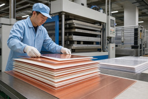
Isola IS415 PCB fabrication follows a controlled high-Tg FR-4 multilayer process, with special attention to material traceability, inner-layer dryness, resin fill, lamination cure, drilling, and finished-board verification. The exact recipe and Isola IS415 lamination cycle must be validated for the board design against the current Isola IS415 processing guide.
- Incoming material verification: Check the IS415 product designation, lot and shelf-life information, laminate thickness, prepreg construction, copper foil, packaging condition, and required compliance documents. Segregate any material with damaged moisture barriers or unclear traceability.
- Inner-layer imaging and etching: Clean, image, develop, and etch the inner layers using a qualified process. The material is compatible with standard aqueous dry films and common cupric chloride or ammoniacal etching systems. AOI verifies opens, shorts, spacing, and registration before bonding.
- Bond treatment and drying: Apply the approved oxide-alternative or bond-enhancement process. For lead-free work, the processing guidance calls for drying inner layers for at least 120 minutes at 110°C or higher. Control handling time so moisture is not reabsorbed before layup.
- Layup preparation: Arrange the verified cores, prepregs, and copper foils in the released sequence. Confirm glass style, ply count, copper orientation, tooling, cleanliness, and stack symmetry. A layup traveler prevents a visually similar prepreg from entering the wrong build.
- Vacuum lamination: Press the book with a qualified IS415 cycle that controls heat ramp, pressure timing, cure, and cooling for the actual copper distribution and board thickness. Verify cured thickness, resin fill, registration, and absence of voiding or delamination. The datasheet states that no post-bake is required after pressing.
- Drilling and hole preparation: Drill with controlled tool life, hit count, entry and backup materials, spindle speed, and feed. Inspect hole quality, then use the validated desmear and conditioning sequence to expose clean copper interfaces without excessive resin or glass damage.
- Metallization and pattern plating: Deposit electroless copper and electroplate to the specified finished hole-wall and surface copper. Monitor bath condition and use cross-sections or coupons to verify plating distribution, barrel integrity, and layer-to-layer connection quality.
- Outer-layer definition and finishing: Image and etch the external circuitry, apply solder mask and legend, then deposit the specified surface finish. AOI, dimensional checks, and finish-thickness controls identify defects before final routing.
- Final verification: Perform electrical test, controlled-impedance testing where specified, visual inspection, dimensional inspection, and representative microsection analysis. Review certificates, lot traceability, and test records against the purchase order before release.
Process capability should be judged from the finished construction rather than the laminate alone. Thick boards, fine holes, high aspect ratios, heavy copper, sequential lamination, or very tight impedance tolerances require additional process review and may need dedicated qualification coupons.
What Factors Affect the Cost of an IS415 PCB?
PCB cost is driven by material utilization, construction complexity, manufacturing yield, verification requirements, quantity, and lead time. A reliable quotation requires the complete fabrication package; a board outline and layer count are insufficient.
- Material availability: Nonstock core thicknesses, prepreg glass styles, copper profiles, or special sheet sizes may increase procurement time and minimum order quantities.
- Layer count and board thickness: More layers add imaging, inspection, layup, drilling, plating, and yield exposure. Thick boards may also require conservative drilling and plating controls.
- Copper weight and distribution: Heavy copper increases raw material use, etching difficulty, resin-fill demand, and spacing constraints.
- Hole and interconnect design: Small holes, high aspect ratios, blind or buried vias, backdrilling, and sequential lamination add process steps and verification.
- Signal-integrity requirements: Tight impedance tolerances, lower-profile copper, coupons, reports, and insertion-loss testing increase setup and test effort.
- Panel utilization: Board dimensions, routing rails, coupons, array design, and defect allowances determine how efficiently an IS415 sheet is used.
- Surface finish and inspection: Finish type, controlled thickness, microsections, thermal testing, CAF-related qualification, or special documentation affect total cost.
- Quantity and schedule: Prototype tooling and setup are distributed across fewer boards, while expedited material and production slots carry additional cost or availability risk.
Reduce cost without weakening reliability by using stocked constructions, simplifying via structures, improving panel utilization, and setting achievable impedance tolerances early. Separate mandatory requirements from negotiable ones before requesting a quotation.
Why Choose EBest Circuit as Your Isola IS415 PCB Manufacturer?
Working with EBest Circuit helps you reduce PCB respins, avoid late material substitutions, shorten technical communication, and carry an approved stackup and test plan from prototype to production.
- Reduce redesign cost with Free DFM: We review Gerber or ODB++ data, drill files, annular rings, copper spacing, board thickness, and manufacturability risks before production. You receive actionable feedback while changes are still less expensive to make.
- Keep the approved IS415 construction unchanged: Before production, we verify the laminate, prepreg, glass style, copper foil, and required thickness against the approved stackup. Any proposed material substitution requires approval and updated impedance and reliability checks.
- Improve first-build impedance accuracy: Stackup and controlled-impedance requirements are reviewed together with pressed dielectric thickness, copper weight, trace geometry, and coupon needs. This reduces avoidable back-and-forth between your layout team and the PCB factory.
- Move more smoothly from prototype to volume: The approved stackup, material definition, fabrication notes, and verification requirements can remain tied to the project record, reducing variation when repeat orders or mass production begin.
- Receive verification matched to your risk: AOI, electrical testing, impedance measurement, dimensional inspection, and microsection requirements can be defined according to the board design instead of relying on a generic final inspection.
- Simplify project coordination: When needed, PCB fabrication can be coordinated with component sourcing, PCB assembly, inspection, programming, testing, and box-build requirements through one communication path.
- Get a clearer quotation and lead-time assessment: We identify nonstandard material, special stackup, test, panel-utilization, and schedule requirements before quoting, making proposals easier to compare on the same technical basis.
For a technical review and quotation, send your Gerber or ODB++ files, target stackup, impedance table, IS415 material requirements, quantity, test requirements, and delivery target.
FAQs About Isola IS415 PCB Material
Q1: Does a 200°C Tg mean an IS415 PCB can operate continuously at 200°C?
A1: No. Tg describes the glass transition region of the resin system; it is not the allowable continuous operating temperature of a finished PCB. The datasheet lists a Relative Thermal Index of 130°C, while the final product limit also depends on copper, solder mask, surface finish, components, assembly, mechanical loading, and certification conditions. Establish the real service-temperature profile and qualify the completed assembly accordingly.
Q2: Is IS415 a halogen-free PCB material?
A2: Do not assume halogen-free status from the IS415 name or high-Tg rating. The supplied datasheet does not establish every project-specific halogen requirement. State the required test standard and limits on the purchase order, then request current compliance documentation for the exact material construction.
Q3: Can IS415 be used in a hybrid PCB stackup with another laminate?
A3: A hybrid build may be possible, but it requires technical validation. Resin systems differ in Dk, Df, CTE, cure behavior, flow, adhesion, drilling response, and moisture characteristics. Review material compatibility, the press cycle, bonding interfaces, finished dielectric thickness, impedance, warpage, and UL implications. Validate a representative coupon or prototype before volume production.
Q4: How many assembly rework cycles can an IS415 PCB tolerate?
A4: There is no universal safe rework-cycle count for every IS415 assembly. The limit depends on local peak temperature, dwell time, heating method, board thickness, copper balance, via structure, component mass, moisture condition, and prior reflow exposure. Define an approved rework profile and maximum exposure count for the actual assembly. For high-reliability products, inspect representative reworked boards for pad damage, delamination, measling, hole-wall cracks, and electrical continuity.
Q5: Which copper foil should be selected for a high-speed IS415 PCB?
A5: Choose copper foil from the channel-loss, adhesion, availability, and fabrication requirements. The IS415 offering includes HTE Grade 3 and RTF options. A lower-profile surface can reduce conductor loss at high frequency, but the benefit depends on trace geometry, frequency, length, and the complete loss budget. Confirm the foil model with the fabricator and include copper roughness in field-solver or channel-simulation work.
Q6: How should IS415 prepreg be stored and handled?
A6: Keep prepreg sealed, traceable, and within the supplier’s specified temperature, humidity, shelf-life, and out-time limits. Record the lot, date removed from controlled storage, exposure time, and any conditioning before use. Damaged packaging, condensation, or uncontrolled exposure can affect resin flow and lamination quality. The current Isola storage guidance and the fabricator’s approved material-control procedure should govern each production lot.
Q7: Can IS415 be used in a sequential-lamination or HDI construction?
A7: It can be considered, but the complete build must be qualified. Review the number of lamination cycles, cumulative thermal exposure, resin fill around buried features, dielectric-thickness control, drilling conditions, copper adhesion, and registration. Approve the construction only after the proposed press cycles and representative coupons demonstrate the required reliability.
Q8: How can you verify that genuine IS415 material was used?
A8: Specify material traceability as a purchase requirement. Request the certificate of conformance or agreed material documentation, supplier and product identification, lot traceability, laminate and prepreg labels, and the approved stackup record. The receiving and layup travelers should connect those records to the manufacturing lot. If program risk justifies it, include customer source restrictions or additional document review before production begins.
Q9: Is IS415 suitable for high-voltage PCB designs?
A9: Material electrical strength alone cannot approve a high-voltage board. The datasheet lists electric strength and insulation properties for tested laminate conditions, but the finished design must also satisfy creepage, clearance, conductor spacing, contamination level, coating, altitude, moisture, and applicable safety-standard requirements. Validate the actual board construction at the required working and test voltages.
Q10: How should an IS415 PCB be qualified for repeated lead-free reflow?
A10: Use a representative finished board or coupon and reproduce the intended thermal exposure. Define the peak temperature, time above liquidus, number of reflow and rework cycles, preconditioning, and acceptance limits. After exposure, use electrical testing, microsections, and interconnect-stress or thermal-cycling tests as required to check for delamination, barrel cracking, pad lifting, and resistance change.
Send Gerber or ODB++ data, the proposed stackup, impedance table, IS415 construction, copper weights, quantity, and test requirements for review and quotation. Include BOM and assembly requirements when applicable, plus the delivery target and required certificates. Submit the package to sales@bestpcbs.com so manufacturability, verification planning, and material supply can be checked before production.
You may also like





Tags: IS415 Datasheet, IS415 PCB Fabrication, IS415 PCB Stackup, Isola IS415 PCB Material