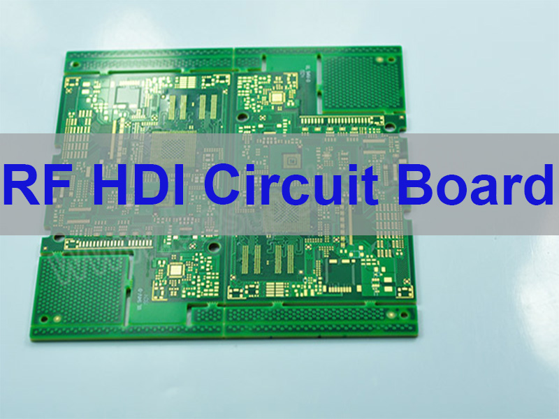
Why choose China for fine line PCB production? This guide mainly discover fine line PCB manufacturers list, how to choose Chinese fine line PCB manufacturer and recommended manufacturer.
Are you troubled with these problems?
- How to ensure signal transmission stability when line width accuracy is insufficient?
- How to balance cost and quality control for multi-layer boards with low yield rates?
- How to guarantee on-time project delivery when lead times are frequently delayed?
As a Chinese fine line PCB manufacturer, EBest Circuit (Best Technology) can provide you service and solutions:
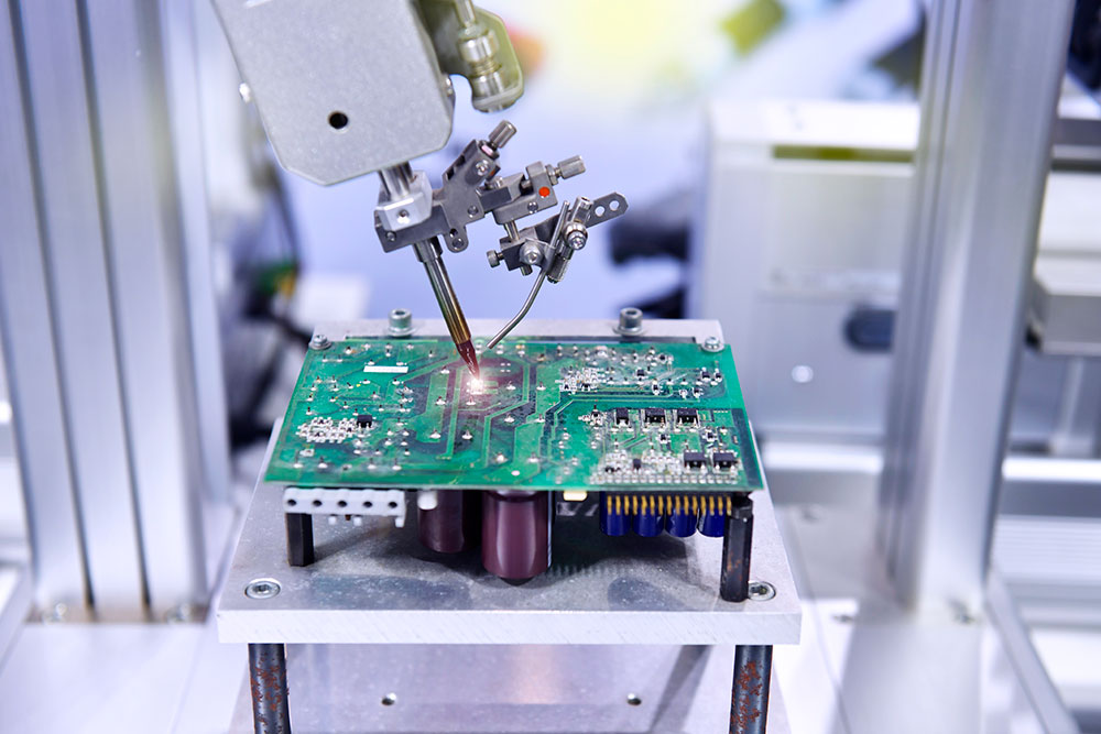
- High-Precision Manufacturing: Utilizing micron-level etching technology to achieve line width tolerance of ±0.01mm, significantly enhancing signal integrity.
- End-to-End Quality Control: Implementing 12 rigorous inspection stages from raw materials to finished products, maintaining yield rates above 99% while reducing rework costs.
- Agile Delivery System: Flexible production lines support 72-hour prototype delivery, cutting mass production cycles by 30%, with priority scheduling for urgent orders.
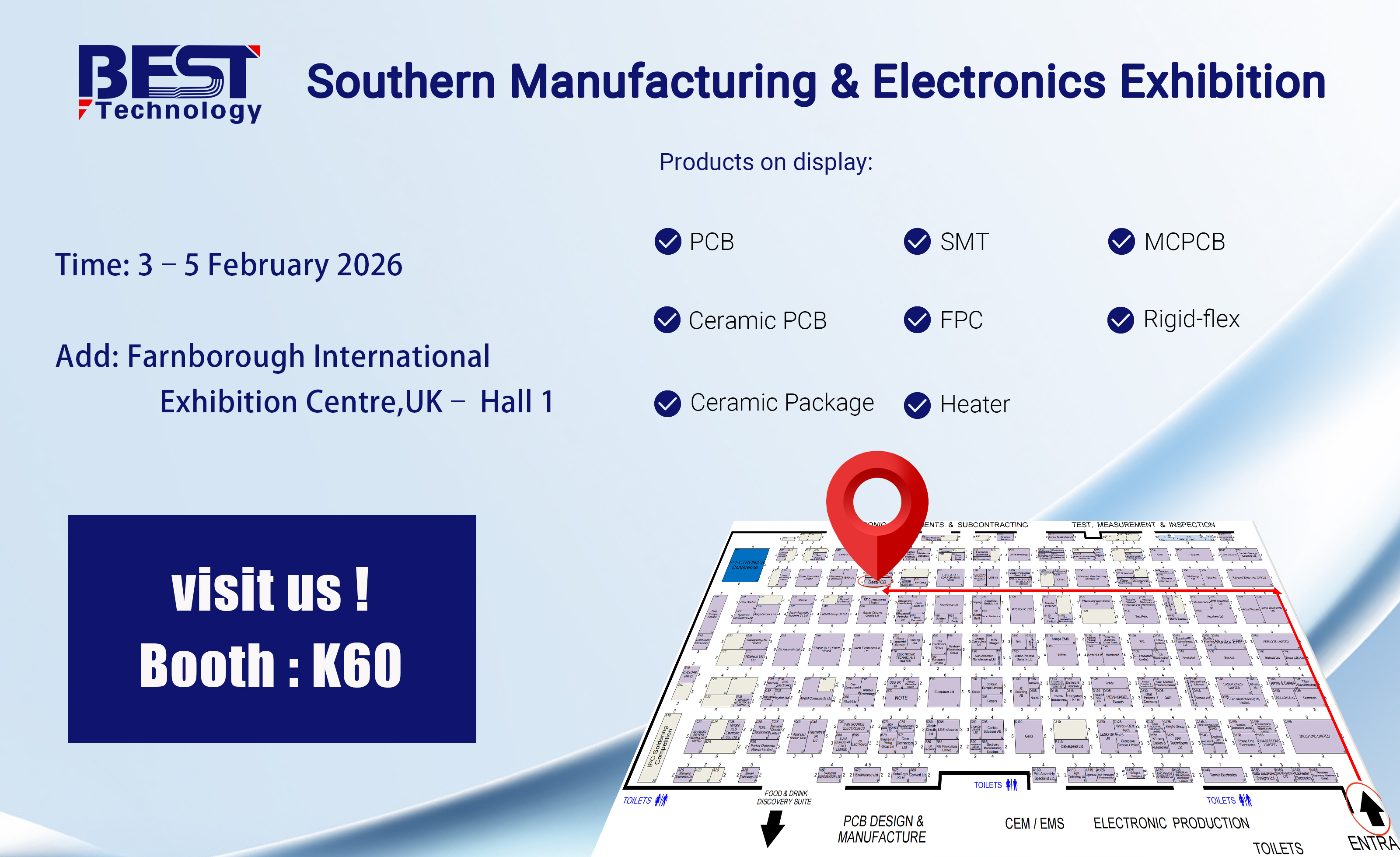
Welcome to contact us if you have any request for fine line PCB: sales@bestpcbs.com.
Why Choose China for Fine Line PCB Production?
Benefits of Chinese fine line PCB manufacturer:
Significant Cost Competitiveness
- China’s mature PCB industry chain ensures abundant and transparently priced raw materials (like copper foil,) and large-scale production capabilities, reducing per-unit manufacturing costs by 20%-40% compared to Europe and the U.S. For fine-line PCBs (line width/spacing ≤100μm), Chinese manufacturers optimize processes like laser direct imaging (LDI) and via-filling plating to further minimize yield loss costs, making it ideal for low-volume, multi-variety prototype verification.
Leading Technical Implementation Capability
- Chinese leading PCB companies have achieved mass production of 75μm line width, with some advanced manufacturers supporting 50μm-class fine-line manufacturing. Combined with high-density interconnect (HDI) and embedded component technologies, they meet high-precision design requirements for consumer electronics, medical devices, and 5G communications. Engineers can directly access Chinese manufacturers’ process databases to rapidly validate design feasibility, avoiding repeated modifications due to process limitations.
Fast Supply Chain Response
- China boasts the world’s most complete PCB supporting ecosystem, with over 80% of processes (from substrates to plating chemicals, equipment to testing services) completed domestically. This “one-stop” supply chain enables 7-10 day rapid prototyping and 15-20 day small-batch delivery, shortening lead times by over 30% compared to Southeast Asian and European/American suppliers, aligning with fast-paced R&D cycles.
Strict Quality Control System
- Mainstream Chinese PCB manufacturers hold international certifications such as ISO 9001, IATF 16949, UL, and some have obtained NADCAP aerospace certification. Full-process controls including AOI optical inspection, flying probe testing, and cross-section analysis keep fine-line defect rates ≤0.1%. Third-party audits are supported to ensure compliance with EU RoHS, REACH, and other environmental standards, reducing compliance risks for overseas clients.
Flexible Customization Services
- Chinese manufacturers excel in handling “non-standard” requirements, such as specialty substrates (high-frequency/high-speed materials), irregular-shaped boards, and rigid-flex boards. Value-added services include design rule checks (DRC), design for manufacturability (DFM) analysis, English technical documentation support, real-time progress tracking, and 24-hour technical assistance, minimizing cross-time zone communication costs and boosting development efficiency.
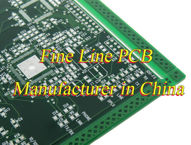
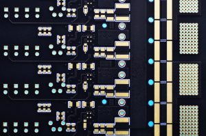
Fine Line PCB Manufacturer in China
Finest Printed Circuit Board Ltd
- Service: Offers HDI PCB, multi-layer boards, impedance control boards, blind/buried via boards, etc., covering one-stop manufacturing from prototypes to mass production.
- Advantages: Minimum line width/spacing of 3mil (0.075mm), supports 3mil microvias, holds UL, ISO 9001, and ISO 14001 certifications, suitable for high-precision and high-reliability designs.
Fastline PCB
- Service: Specializes in high-frequency multi-layer boards, aluminum substrates, HDI, rigid-flex boards, thick copper boards, and PCBA assembly, providing “one-stop PCB solutions.”
- Advantages: Over 70% of products exported to 40+ countries, with extensive experience in telecommunications, industrial control, aerospace, and other fields.
JLCPCB
- Service: Provides high-precision multi-layer boards, HDI boards, impedance control boards, and PCBA, featuring real-time online quoting and order tracking systems.
- Advantages: Employs advanced processes for fine line width/spacing, supports high-density interconnect designs; cost-effective, ideal for startups and small-to-medium design teams.
Shenzhen Core Hecheng Electronic Technology Co., Ltd.
- Service: Mainly offers HDI boards, flexible boards, metal substrates, rapid prototyping, mass production, and provides PCBA assembly and component sourcing.
- Advantages: Dedicated HDI production line with layer capacity of 1-48 layers, minimum line width/spacing of 3-4mil, impedance control accuracy of ±10%.
Shenzhen Goldmate Electronics Co., Ltd.
- Service: Covers high multi-layer PCB, HDI, rigid-flex boards, high-frequency high-speed boards, and full PCBA services.
- Advantages: Holds factory audit supplier qualifications, certified to ISO 9001:2015 and ISO 14001, with a robust quality management system.
How to Select A Reliable Chinese Fine Line PCB Manufacturer?
A practical guide to how to choose a reliable fine line PCB manufacturer in China:
1. Verify Qualifications & Certifications
- International Standards Certification: Prioritize manufacturers with ISO 9001 (Quality Management), ISO 14001 (Environmental Management), IATF 16949 (Automotive Electronics, mandatory implementation by 2025), AS9100D (Aerospace), and IPC-6012/6018 certifications. Validate certificates via official platforms (e.g., UL Certificate Verification Portal). Avoid temporary/provisional certificates labeled “preliminary audit passed.”
- Industry-Specific Compliance: For high-frequency PCBs, confirm IPC-6018 (microwave substrate performance) compliance; for HDI boards, ensure IPC-6012 Class 3 (blind/buried vias & microvia filling) adherence. Environmental compliance requires RoHS 3.0 reports and REACH SVHC substance declarations.
2. Evaluate Technical Capabilities & Equipment
- Line Width/Spacing Capability: Request SEM micrographs and electrical test data to verify ≥95% yield for 2-3mil line/space. LDI equipment must support 0402 component precision exposure; electroplating lines require pulse plating for uniform copper deposition.
- Advanced Equipment: Check for dual-panel placement machines, AOI with 3D SPI (solder paste thickness) and X-ray laminography (for BGA solder joint inspection). Material compatibility includes high-frequency substrates (e.g., Rogers RO4350B, Taconic TLC series) and low-loss laminates.
3. Review Production Experience & Case Studies
- Industry Experience: Demand ≥3 anonymized mass production cases with client names (redacted), product models, production volumes, and yield data. Verify details via third-party test reports (SGS/TÜV) or direct communication with case engineers.
- Sample Testing: Free samples must include impedance control reports (e.g., 100Ω±10% differential impedance), thermal cycling (-55°C~125°C for 1,000 cycles), salt spray (96h no corrosion), and electrical tests (insulation resistance ≥100MΩ). Pre-mass production requires First Article Inspection Reports (FAIR) with Cpk ≥1.33.
4. Communication & Collaboration Efficiency
- Language & Time Zone Support: Dedicated English technical teams with 24/7 availability via platforms like Microsoft Teams. Real-time screen sharing and document collaboration tools ensure accurate design parameter transmission.
- Design Support: DFM analysis includes trace spacing optimization, impedance matching calculations, manufacturability assessments (min. annular ring, pad size), and testability design (test point layout). Gerber file validation tools (e.g., Valor NPI) minimize design iterations.
5. Quality Control & Traceability Systems
- Full-Process Control: Require records from raw material incoming inspection (e.g., ±5% laminate thickness tolerance), in-process SPC (copper thickness Cpk ≥1.67), 100% electrical testing (flying probe), and outgoing inspection (ISTA 2A packaging).
- Traceability: ERP-integrated batch tracking links raw material lots, equipment IDs, operator info, and key process parameters (exposure energy, plating current). QR/RFID tags enable rapid traceability.
6. Cost Transparency & Delivery Management
- Transparent Quoting: Itemized quotes detailing laminate costs, processing fees (drilling/plating), testing (AOI/X-ray), and logistics (DHL/FedEx). Clarify tooling costs inclusion to avoid hidden charges.
- On-Time Delivery: Contracts specify lead times (7 days for prototypes, 14 days for mass production) with daily penalties (0.1%-0.5% of order value) for delays. Logistics include multi-modal solutions (air/sea/rail) with real-time tracking.
7. On-Site Audits & Supply Chain Transparency
- Factory Visits: Audits focus on cleanroom classification (Class 10,000), equipment maintenance logs (calibration reports), employee training certifications (IPC-600), and environmental facilities (wastewater treatment, emissions monitoring).
- Supply Chain Disclosure: Key suppliers must provide material test reports (copper tensile strength, resin Tg). Raw material traceability ensures compliance with Conflict Minerals regulations.
8. After-Sales Support & Technical Assistance
- Technical Assistance: 24/7 support with rapid response (2h initial feedback), process troubleshooting (e.g., pad lift repair guidelines), and remote diagnostics (video conference defect analysis).
- Warranty: Formal contracts define 1-2 year warranty periods with free repair/replacement for defects.
- Long-Term Partnership: Support low-volume trials (50+ pieces), 24h expedited prototyping, and quarterly process improvement workshops to foster stable collaborations.
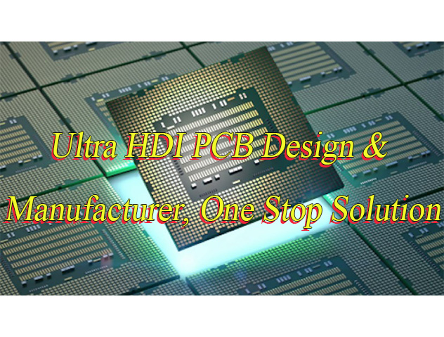
Why Choose EBest Circuit (Best Technology) as Fine Line PCB Manufacturer?
Reasons why choose us as fine line PCB manufacturer in China:
- Free DFM Design Optimization Service: Provide professional free DFM (Design for Manufacturing) analysis to identify design defects early, reduce modification costs and time, ensure one-time design success, and accelerate product launch.
- 1 Piece MOQ: Support single-piece orders with no minimum quantity restrictions, ideal for designers’ prototype verification and small-batch trial production, reducing early development costs and risks.
- Full Turnkey Solution: Offer seamless one-stop services from prototype design, rapid prototyping, mass production to SMT assembly, eliminating the need for clients to coordinate with multiple suppliers, saving communication costs and time, and enhancing project efficiency.
- Highly Competitive Pricing: Deliver industry-leading price levels through scaled production and lean supply chain management, particularly outstanding cost-effectiveness for bulk orders, helping overseas clients control project costs.
- Rapid Prototyping: Conventional orders feature significantly faster turnaround times than industry averages, while urgent orders benefit from 24-hour rapid prototyping services to meet overseas designers’ needs for fast iteration and agile development, securing market opportunities.
- Rigorous Quality Control System: Adopt internationally standardized quality control processes, certified by ISO9001, AS9100D (aerospace), ISO13485 (medical), ROHS, REACH, and other authoritative standards, with full traceability from raw materials to finished products, guaranteeing worry-free product quality.
- Experienced Engineer Team Support: Composed of seasoned engineers with an average of 19 years of experience, the team provides comprehensive technical support from design consultation, process optimization to problem resolution, deeply understanding client technical requirements and solving complex engineering challenges.
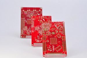
Our Fine Line PCB Manufacturing Capabilities
| Item | Capabilities |
| Layer Count | 1 – 32 Layers |
| Max Board Dimension | 24*24″ (610*610mm) |
| Min Board Thickness | 0.15mm |
| Max Board Thickness | 6.0mm – 8.0mm |
| Copper Thickness | Outer Layer:1oz~30oz, Inner Layer:0.5oz~30oz |
| Min Line Width/Line Space | Normal: 4/4mil (0.10mm); HDI: 3/3mil (0.076mm) |
| Min Hole Diameter | Normal: 8mil (0.20mm); HDI: 4mil (0.10mm) |
| Min Punch Hole Dia | 0.1″ (2.5mm) |
| Min Hole Spacing | 12 mil (0.3mm) |
| Min PAD Ring(Single) | 3mil (0.075mm) |
| PTH Wall Thickness | Normal: 0.59mil (15um); HDI: 0.48mil (12um) |
| Min Solder PAD Dia | Normal: 14mil (0.35mm); HDI: 10mil(0.25mm) |
| Min Soldermask Bridge | Normal: 8mil (0.2mm); HDI: 6mil (0.15mm) |
| Min BAG PAD Margin | 5mil (0.125mm) |
| PTH/NPTH Dia Tolerance | PTH: ± 3mil (0.075mm); NPTH: ±2 mil (0.05mm) |
| Hole Position Deviation | ±2 mil (0.05mm) |
| Outline Tolerance | CNC: ± 6mil (0.15mm); Die Punch: ± 4mil (0.1mm); Precision Die: ± 2mil (0.05mm) |
| Impedance Controlled | Value>50ohm: ±10%; Value≤50ohm: ±5 ohm |
| Max Aspect Ratio | 0.334027778 |
| Surface Treatment | ENIG, Flash Gold, Hard Gold Finger, Gold Plating(50mil), Gold finger, Selected Gold plating,ENEPIG, ENIPIG; HAL, HASL(LF), OSP, Silver Imm., Tin Imm |
| Soldermask Color | Green/White/Black/Yellow/Blue/Red |
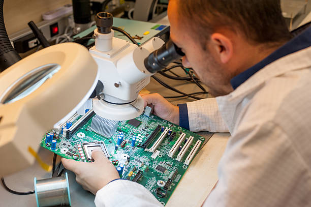
Our Quality Control for Fine Line Printed Circuit Board
1. Appearance & Pattern Inspection
- Automated Optical Inspection (AOI): Conduct AOI scanning after etching, solder mask, and other critical processes to detect pattern defects in fine lines such as opens, shorts, notches, and burrs.
- Solder Mask & Silkscreen Inspection: Verify uniform solder mask coverage without bubbles, peeling, and clear, accurately positioned silkscreen to prevent welding/identification issues.
- Surface Defect Inspection: Visual or magnified inspection for scratches, exposed copper, oxidation, contamination, and other surface defects.
2. Electrical Performance Testing
- Open/Short Testing: Validate network connectivity via flying probe or in-circuit test (ICT) to ensure no opens or shorts.
- Impedance Testing: Sample high-speed fine lines and measure characteristic impedance using time-domain reflectometry (TDR) to confirm compliance with design values (typically ±10%).
- High-Voltage & Insulation Resistance Testing: Apply high voltage to check interlayer insulation strength and measure insulation resistance to prevent leakage or breakdown.
3. Dimensional & Structural Verification
- Line Width/Spacing Measurement: Use microscopes or image measurement systems to spot-check fine line width/spacing against design tolerances (e.g., ±0.02 mm).
- Layer-to-Layer Alignment: Perform cross-sectional analysis to check multi-layer board alignment and prevent impedance anomalies or shorts due to misregistration.
- Hole Position & Diameter Inspection: Confirm drilling position, hole size, and hole wall quality to avoid metallized hole fractures or pad peeling.
4. Process & Material Inspection
- Plating Thickness Measurement: Use X-ray fluorescence to check uniformity of copper, immersion gold/tin, and other surface finish thickness.
- Solderability Testing: Conduct solder float or wetting balance tests to confirm pad solderability and prevent solder joint defects.
- Cleanliness Inspection: Test for ionic contamination or extract resistivity to detect residual flux/ion pollutants and ensure long-term reliability.
5. Environmental & Reliability Validation
- Thermal Shock Testing: Subject PCBs to high-low temperature cycles (e.g., -55°C to +125°C) to evaluate fine line/substrate adhesion and hole wall thermal resistance.
- Microsection Analysis: Prepare vertical/horizontal sections to observe inner-layer copper thickness, resin fill, hole copper integrity, and other microstructural features.
Our Lead Time for Fine Line PCB Prototyping
| Layers | Normal Service | Fastest Service |
| 1 | 7 Days | 24 H |
| 2 | 8 Days | 24 H |
| 4 | 10 Days | 48 H |
| 6 | 10 Days | 72 H |
| 8 | 12 Days | 72 H |
| ≥10 | TBD | TBD |
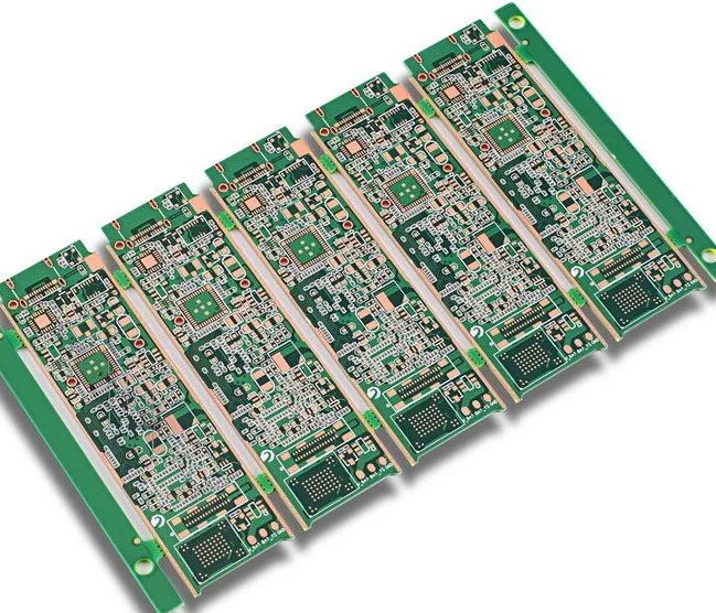
Case Studies of Fine Line PCB We Made Before
Case: High-End Smartphone Motherboard (10-Layer 1st-Order HDI Board)
Client Requirements:
A smartphone brand aims to launch a new generation of slim flagship devices, requiring high-density routing, high-speed signal transmission, and multi-chip integration within an extremely small motherboard area. Traditional PCBs cannot meet signal integrity and thermal dissipation requirements, necessitating the use of Fine Line HDI technology with minimum line width/spacing below 100μm and extremely low high-frequency signal loss and crosstalk.
Solution:
Design Phase
- Structure: Adopt 1+8+1 10-layer 1st-order HDI structure, achieving high-density interlayer interconnection through 0.1mm UV laser microvia and 0.25mm mechanical buried hole
- Process: Utilize mSAP (semi-additive process) technology to fabricate fine lines with 0.088mm/0.087mm line width/spacing (approximately 3.5/3.4mil), significantly enhancing routing density.
- Thermal Management: Implement 1OZ thick copper design on power and ground layers, combined with L3-L6 layer local resin plugging to strengthen thermal management and mechanical strength.
Manufacturing Processes
- Laser Drilling: Use UV laser to form 0.1mm microvias, ensuring smooth hole walls without damage to adjacent traces.
- Copper Plating: Fill vias with copper plating to prevent thermal stress cracking caused by gas residues.
- Fine Line Imaging: Employ LDI (laser direct imaging) exposure on dry film photoresist to achieve ±5μm line width tolerance.
- Surface Finish: Select ENIG (electroless nickel immersion gold) as pad surface treatment for chip attachment flatness and soldering reliability.
Verification and Testing
- Signal Testing: Verify impedance consistency via TDR (time-domain reflectometry); high-speed signal line insertion loss and return loss comply with IEEE 802.3 standards.
- Environmental Testing: Pass -40°C to +125°C thermal cycling and 85°C/85%RH high-humidity high-temperature tests, confirming long-term reliability under harsh conditions.
Results:
The HDI motherboard successfully integrates over ten chips including CPU, memory, and RF modules on a 242mm×165mm board surface, achieving approximately 40% routing density improvement and 25Gbps signal transmission rate. Device thickness reduced by 1.2mm, fulfilling the design goals of slim profile, high performance, and high reliability.
How to Get A Quote for Fine Line PCB Project?
All material list required for fine line PCB quote:
- Layer Count: Specify the number of layers (e.g., 4-layer/6-layer/8-layer)
- Material Type: Indicate substrate material (e.g., FR4, high-frequency material, high-Tg material)
- Board Thickness: Precise measurement in millimeters (e.g., 1.0mm/1.6mm)
- Copper Thickness: Inner/outer layer copper weight (e.g., 1oz/2oz)
- Minimum Trace Width and Spacing: Critical parameters (e.g., 3mil/3mil or smaller)
- Surface Finish: Select process (e.g., ENIG/HASL/OSP/immersion silver)
- Solder Mask Color: Specify ink color (e.g., green/black/blue)
- Drilling Requirements: Minimum hole size and blind/buried via needs (e.g., 0.1mm hole size)
- Special Processes: Impedance control/plating process/HDI requirements
- Order Quantity: Clear batch size (e.g., 100 pieces/500 pieces)
- Lead Time Requirement: Specific delivery timeline (e.g., 7 days/10 days)
Please feel free to contact us to get an accurate quote and free DFM for your PCB project: sales@bestpcbs.com.