

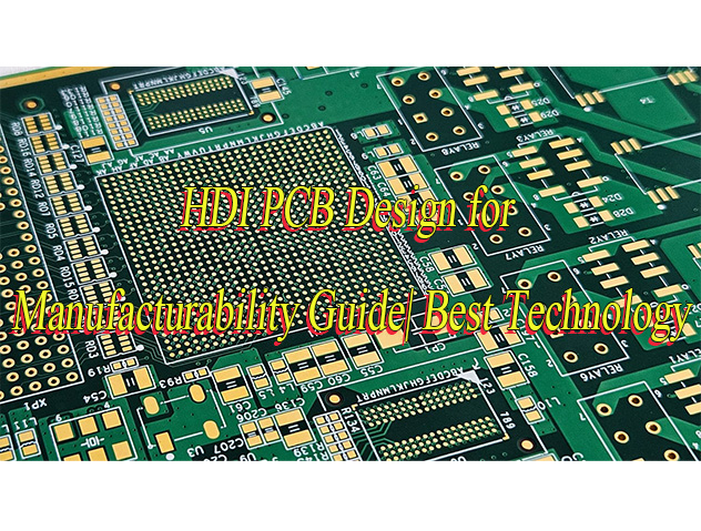
How to design HDI PCB for manufacturability? Let’s discover material selection, layer stackup, design optimization, thermal solutions, testing methods , cost reduction methods about HDI PCB design manufacturability.
Are you struggling with these HDI PCB design issues?
- Do microvia misalignment issues in your HDI PCB cause frequent short circuits or open failures during production?
- Is high-density routing causing uncontrolled crosstalk that compromises product performance and fails customer validation?
- Does disjointed design verification processes extend your time-to-market, missing critical market windows?
As a HDI PCB Manufacturer, EBest Circuit (Best Technology) can provide you service and solutions:
- Free DFM Prediction: Leverage our 20-year manufacturing database to identify 20+ manufacturability risks (e.g., microvia placement, trace/space tolerances) upfront with actionable reports.
- Manufacturability-Optimized Design: Tailor HDI-specific routing topologies and hole placement strategies to reduce costs by ≥30% while improving performance consistency by ≥20%.
- Rapid Validation Cycle: Complete end-to-end design-to-DFM feedback in 72 hours, ensuring seamless production alignment and accelerated market entry without compromising quality.
Welcome to contact us if you have any request for HDI PCB Board design, manufacturing and assembly: sales@bestpcbs.com.
Material Selection Guide for HDI PCB Manufacturability Design
A guide to how to choose material for HDI PCB for manufacturability:
1. High-Frequency & Thermal Management Balance Design for Substrate Selection
- Core Parameters: For high-frequency scenarios, prioritize substrates with Dk ≤3.5 and Df ≤0.005 (e.g., PTFE ceramic-filled substrates). 5G millimeter-wave radar requires nanocomposite materials with Df <0.002.
- Thermal Stability: Automotive electronics demand Tg ≥170°C (e.g., polyimide substrate Tg >280°C). CTE must match chip packaging layers (6-8ppm/°C) to prevent delamination from thermal expansion differences.
- Special Environmental Requirements: Industrial control equipment requires chemical corrosion resistance, low moisture absorption (<0.3%), and high hardness (Shore D80+). Aerospace-grade substrates must pass vacuum outgassing tests (<1% mass loss).
2. Copper Foil Thickness Gradient Design Strategy
- Fine-Line Circuits: 0.5oz (17.5μm) copper foil suits HDI with line widths <0.1mm, paired with electroplating thickening for reliable connections.
- High-Current Pathways: Power modules use 2-3oz (70-105μm) copper foil. Current capacity is calculated as line width ×1.2A/mm, with 20% margin for transient surges.
- Flexible Circuits: Ultra-thin rolled copper foil (9-12μm) paired with PI substrate. Bend radius must be ≥5× copper thickness to avoid fatigue fractures. Thick copper boards require stepped etching to control undercut.
3. Solder Mask Material Process Compatibility Selection
- LPI Liquid Photoimageable Solder Mask: Suitable for complex surfaces/microvia filling. Withstands thermal shock (≥3 cycles at 288°C) and chemical plating resistance.
- Dry Film Solder Mask: Preferred for microvias <0.1mm diameter. Excellent wear resistance. Exposure energy must be controlled (80-120mJ/cm²) to prevent incomplete development.
- Environmental Compliance: Meets RoHS/REACH standards. Low VOC emissions (<50g/m²). Lead-free solder compatibility verified via SIR (Surface Insulation Resistance) testing.
4. Laminate Material & Process Synergy Optimization
- Prepreg Selection: FR-4 (general-purpose, Tg 130-140°C). High-speed signal applications use Megtron 6 (Dk=3.7, Df=0.009) or Nelco N7000-2HT (Tg>200°C).
- RCC Resin-Coated Copper: Applied in ultra-thin HDI (<0.4mm thickness) to minimize void defects from uneven resin flow during lamination.
- Process Control: Vacuum lamination pressure 300-400psi. Temperature profile segmented (preheat 120°C/1h, main press 180-200°C/2h, post-press 150°C/1h). X-ray inspection ensures microvia fill ratio ≥95%.
5. Surface Finish & Metallization Process Selection
- ENIG (Electroless Nickel Immersion Gold): Ideal for high-frequency RF connectors. Au 2-5μm, Ni 3-7μm. Excellent corrosion resistance but higher cost.
- ENEPIG (Electroless Nickel Electroless Palladium Immersion Gold): Adds palladium layer for enhanced solder joint reliability. Suitable for high-reliability medical/automotive electronics. Pd thickness 0.05-0.2μm.
- OSP (Organic Solderability Preservative): Cost-effective solution for consumer electronics. Thickness 0.3-0.8μm. Limited shelf life (6 months) and sensitive to humidity/heat.
6. Sustainable & Eco-Friendly Design Strategies
- Material Recycling: Use bio-based resins (e.g., castor oil-modified epoxy) and peelable solder masks. Complies with IEC 61249-2-21 halogen-free standards.
- Carbon Footprint Reduction: Prioritize local suppliers to minimize transport emissions. Adopt water-based cleaning processes to reduce VOC emissions.
- Compliance Certifications: Must pass UL 94 V-0 flammability rating, IPC-4101 substrate standards, and customer-specific reliability tests (e.g., THB 85°C/85%RH for 1000h).
7. Customized Solutions for Specialized Applications
- Aerospace: Use low Dk/Df LCP substrates (Dk=2.9, Df=0.002). Validate radiation resistance (>100kGy) and extreme temperature performance (-55°C~150°C).
- Medical Implants: Biocompatible substrates (e.g., PI/PEEK composites). Pass ISO 10993 biocompatibility tests. Verify corrosion resistance in bodily fluids and long-term reliability.
- High-Reliability Power: Thick copper foil (>3oz) paired with thermal conductivity >3W/m·K substrates. Thermal simulation confirms hotspot temperature <85°C to prevent localized overheating failures.
Layer Stackup Design Principles for HDI PCB Manufacturability Design
Below are layer stackup design principles for HDI PCB manufacturability design:
1. Layer Count and Complexity Balance
- Demand-Driven Layer Design: Layer count is determined by signal network density, BGA pin pitch (e.g., ≥6 layers for 0.4mm/0.3mm pitch), number of power planes, and high-speed signal integrity requirements (e.g., ≥100MHz requires dedicated layers). Common ranges are 4-12 layers. High-density BGAs (e.g., 1000+ pins) require increased layer counts for routing redundancy to avoid signal cross-interference.
- Thickness-Layer-Reliability Triangular Constraints: Low-dielectric-constant (Dk=3.0-3.8) materials with 3-5mil thickness enable one layer per 2-3mil thickness increase, but thermal expansion coefficient (CTE≤17ppm/℃) and mechanical strength must be verified to prevent delamination or warpage during thermal cycling (-40℃~125℃).
- Cost-Benefit Analysis: Each 2-layer increase raises costs by 15-20%. SI/PI co-simulation verifies layer necessity to avoid overdesign.
2. Material Selection and Supplier Collaboration
- Pre-Manufacturing Verification: Confirm material library compatibility (e.g., Panasonic R-5775, ITEQ EM528), minimum process capabilities (trace width/spacing ≥3mil, microvia diameter ≥75μm), and cost models with manufacturers. Prioritize IPC-4101 certified materials.
- Impedance Control Closure: Use Polar Si9000 for impedance modeling with Dk/Df data (e.g., Df≤0.005 for high frequencies) to ensure single-ended 50Ω±10% and differential 100Ω±10% tolerances, validated via TDR testing.
- High-Frequency Material Selection: RF/mmWave (>28GHz) designs use RO4835 (Dk=3.48, Df=0.0027) or TU-872 (Dk=3.9, Df=0.008) to minimize dielectric loss.
3. Microvia Technology and Stack Types
Microvia Structure Adaptation:
- Blind Vias: Surface to Layer 2/3 for BGA escape routing, with depth tolerance ±8μm.
- Buried Vias: Internal layer interconnection (e.g., L3-L5), reducing surface usage but requiring laser drilling + copper plating fill, increasing costs by 10-15%.
- Stacked Microvias: For Type III HDI (ELIC), requiring ±25μm alignment accuracy, boosting routing density by >30%.
- Staggered Vias: Higher mechanical reliability for automotive/industrial applications but limited density improvement.
Typical Stack Configurations:
- 1+N+1: Mainstream for consumer electronics, supporting blind/buried vias with optimal cost-benefit ratio.
- 2+N+2: Common for telecom equipment, enhancing routing density with two blind/buried via passes.
- Type III (ELIC): Layer-to-layer interconnection, increasing density by 50% but raising costs by 30-40%, requiring high-precision laser drilling.
4. Power and Ground Plane Planning
- Signal Layer-Plane Coupling: Adopt S-G-S-P (Signal-Ground-Signal-Power) structure to ensure signal layers are ≤5mil from reference planes, reducing crosstalk (<30dB@1GHz). Power-Ground Plane Pairing: Main power and ground planes spaced 2-4mil apart form planar capacitance (>10nF/cm²), suppressing power noise (<50mVpp).
- Split Plane Compensation: Cross split power planes with 0201 decoupling capacitors (≤0.1μF) to maintain return path continuity.
5. Symmetry and Thermal Management
- Symmetrical Laminate Design: Dielectric thickness deviation <5%, copper foil thickness deviation <10% to prevent warpage (≤0.75%).
- Thermal Relief Design: BGA pad areas use cross-shaped thermal pads (30-50% open ratio) to reduce soldering thermal stress.
- CTE Matching: Core materials (e.g., FR4) and prepregs (e.g., 106) must have CTE differences <5ppm/℃ to minimize thermal cycling stress.
6. Manufacturing Rules and Tolerance Control
- Design Rule Alignment: Follow manufacturer DRC (e.g., trace width ≥3mil, spacing ≥3mil, microvia pad ≥hole diameter +8mil), with tolerance allowances (layer alignment ±2mil, etching ±20%).
- DFM/DFA Verification: Use Valor NPI or Altium Designer DFM tools for rule checks to identify shorts and impedance deviations early.
- Tolerance Chain Management: Account for laminate thickness fluctuations (±10%) and etching variations (±0.5mil) to maintain impedance tolerances.
7. Documentation and Supply Chain Collaboration
- Standardized Documentation: Output stack data in IPC-2581 format (including drill tables, impedance specs, BOMs) to reduce communication errors.
- Multi-Supplier Adaptation: Provide stack variants (e.g., alternative materials, microvia adjustments) for different manufacturers to ensure seamless prototype-to-production transitions.
- Impedance Test Correlation: Link design-stage Polar Atlas Si test systems to ensure <10% deviation between theoretical models and physical impedance.
HDI PCB Manufacturability Design Process Optimization Strategies
Optimization strategies for HDI PCB manufacturability design process:
Signal and Power Integrity Co-Optimization:
- Precise Impedance Control: Utilize simulation tools such as HyperLynx and Ansys SIwave to calculate trace width, spacing, and dielectric thickness, ensuring ±10% impedance tolerance (e.g., 50Ω single-ended lines, 100Ω differential pairs). A case study from Dingji Electronics demonstrates that impedance continuity design improves signal integrity of 5G modules by 12%.
- Crosstalk Suppression Strategy: Differential pairs adopt tightly coupled design with 0.08mm line width and 0.08mm spacing, maintaining 100Ω±2% impedance and enhancing noise immunity by 15%. Combined with ground via shielding (spacing <0.5mm), crosstalk is reduced to below -70dB.
- Power Distribution Network Optimization: Implement grid-based power planes or multi-point via stitching, paired with decoupling capacitors (e.g., 0402 capacitors around BGA packages) to minimize power noise. For high-frequency scenarios, low-Dk materials like Rogers 4350B reduce signal loss.
Thermal Management Innovation
- High-Power Device Cooling: Copper-filled Via-in-Pad blind vias under BGA chips enhance thermal conductivity. Combined with high-thermal-conductivity substrates like Megtron 6, overall thermal performance improves by over 30%.
- Stack-Up Optimization: An 8-layer symmetric stack-up with alternating signal-ground-power layers routes high-speed signals through inner layers and low-speed signals on outer layers, increasing routing density by 40%. Orthogonal routing (horizontal on top layer, vertical on bottom layer) reduces cross-interference, lowering crosstalk from -45dB to -65dB.
Microvia and Blind/Buried Via Technology Advancements
- Laser Microvia Processing: UV laser drilling (355nm wavelength) achieves 0.1mm blind via diameter with >95% pad alignment accuracy. Electroplated copper-filled blind vias with >98% fill rate reduce impedance from 65Ω to 55Ω, improving return loss by 8dB.
- Blind/Buried Via Configuration Strategy: In 2+N+2 stack-ups, blind vias connect adjacent layers and buried vias connect inner layers. Avoiding excessive lamination steps (e.g., reducing HDI class) lowers manufacturing complexity and costs.
Design for Manufacturability (DFM) Rule System
- Design-Manufacturing Collaboration: Collaborate closely with PCB manufacturers to confirm process capabilities such as minimum trace width/spacing (25μm) and via diameter (0.1mm). AOI/AXI inline inspection catches defects like line width deviations >5μm and via voids >10%.
- Material Selection and Environmental Compliance: Choose low-Dk (3.5-4.0) and low-loss (0.002-0.005) high-frequency laminates with RoHS-compliant materials to minimize environmental impact.
- Simulation-Driven Validation: Perform signal integrity, power integrity, and thermal analysis during design to identify issues like reflection loss, voltage drop, and thermal hotspots. An 8-panel case showed 25% improvement in 10GHz signal eye opening and one-order magnitude reduction in bit error rate after layer optimization.
Manufacturing Process and Cost Balancing
- Precision Lamination and Alignment: X-ray positioning with optical compensation achieves <5μm interlayer alignment error and >99.9% via connectivity. Narrow-band bridge designs (1mm width) integrate buried resistors/capacitors (±5% accuracy), saving surface-mount component space.
- Automation and Quality Control: Automated production lines for laser drilling and micro-line etching, coupled with real-time monitoring systems, ensure process stability. Full-flow quality management from raw materials to final inspection lifts yield to >95%.
- Cost Optimization Pathways: Prioritize 1+N+1 or 2+N+2 structures to avoid over-lamination. Via-in-Pad filling reduces routing length and improves routing efficiency. Balance performance and cost by selecting cost-effective substrates (e.g., FR4-high-frequency hybrid laminates) and optimizing stack-up.
Thermal Solutions for HDI PCB Manufacturability Design
High Thermal Conductivity Substrate and Heat Dissipation Layer Design
- Material Selection: HDI PCBs require substrates with thermal conductivity ≥2.0 W/m·K due to high-density interconnection and thin copper foil (≤35μm). For instance, nanoceramic substrates developed by Liebo PCB achieve 2.8 W/m·K thermal conductivity, 9 times higher than traditional FR-4. At 10GHz, the dielectric loss Df<0.001, and CTE=6.5ppm/℃ matches Si chips, eliminating thermal stress under wide temperature ranges. A 5G base station HDI board using aluminum substrate reduced thermal resistance by 40% and junction temperature by 15℃.
- Heat Dissipation Layer Construction: Insert dedicated heat dissipation layers (e.g., thick copper ≥105μm) between signal layers. Thermal via arrays (diameter 0.3mm/pitch 1.0mm) connect top/bottom heat sources to inner heat dissipation layers, forming a 3D heat dissipation network. A vehicle radar HDI board adopted this design, improving continuous working temperature stability by 20%. Combined with high-frequency material hybrid pressing (e.g., Rogers RO4350B Dk=3.48, Df=0.0037 mixed with FR-4), HFSS simulation optimized layer stacking, reducing 28GHz insertion loss by 18% and cost by 22% compared to full high-frequency schemes.
Heat Source Layout and Thermal Isolation Strategies
- Heat Source Distribution Optimization: High-power devices (e.g., CPU, power MOSFET) follow the “heat source dispersion” principle to avoid localized hotspots. A server HDI board placed CPU and memory modules diagonally opposite, with thermal adhesive filling, reducing the maximum temperature difference from 18℃ to 8℃. Processor cores are centered on the chip, surrounded by thermal vias for rapid heat conduction to the package substrate heat sink.
- Thermal Isolation Technology: Set “thermal isolation zones” (width ≥2mm) around heat-sensitive components (e.g., crystals, sensitive ICs) using etched gaps or low-thermal-conductivity materials (e.g., silicone). A medical HDI board implemented this, narrowing critical IC temperature fluctuations to ±3℃. For RF chips, power amplifiers are placed near chip edges with miniature heat sinks, optimizing interconnect layout to reduce high-frequency signal loss and heat generation.
Thermal Via and Heat Dissipation Pad Optimization
- Thermal Via Design: Adopt “thermal via arrays” (density ≥50 vias/cm²) with metalized vias to rapidly conduct heat to inner heat dissipation layers or bottom heat dissipation pads. Simulation shows a communication module HDI board reduced thermal resistance in the via area by 60%. Solid copper-filled vias (0.3mm diameter) achieve 14°C/W thermal resistance, 30% lower than hollow vias.
- Heat Dissipation Pad Enhancement: For high-power devices (e.g., QFN packages), design a 3D thermal structure combining “heat dissipation pad + thermal via + heat dissipation layer”. An LED driver HDI board adopted this, improving pad temperature uniformity by 30% and solder joint reliability by two grades. Additional heat sinks and heat dissipation holes leverage airflow, while integrated micro-fans or liquid cooling systems enable active cooling.
Thermal Simulation-Driven Design Iteration
- Simulation Tool Application: Use ANSYS Icepak, Flotherm, etc., for thermal-electrical coupled simulations to predict temperature distribution and thermal stress accurately. A drone HDI board optimized heat dissipation paths through simulation, reducing critical area temperatures by 12℃ and verifying manufacturing tolerances (e.g., ±0.1mm lamination offset) impact on heat dissipation. Experimental validation (e.g., infrared thermal imaging, thermocouple measurements) calibrates simulation results.
- Iterative Validation Logic: Form a “design-simulation-optimization” loop by adjusting layout, via density, and material parameters based on simulation results. An AI accelerator HDI project reduced peak temperature from 115℃ to 95℃ through three iterations, meeting long-term reliability requirements. CST Multiphysics Studio performs board-level thermal simulation by importing PCB files, automatically setting heat sources, and accelerating simulation speed while ensuring result validity.
Manufacturing Process Synergy Optimization
- Lamination Process Control: Use “low-temperature lamination + vacuum pressing” to prevent thermal degradation of substrate thermal properties. A consumer electronics HDI board optimized this process, reducing interlayer thermal conductivity fluctuations from ±15% to ±5%. Liebo PCB deployed AI-driven electromagnetic simulation tools to reduce routing conflicts by 40% and achieved impedance tolerance of ±5% via TDR dynamic monitoring.
- Surface Treatment and Thermal Interface Materials: Select high-thermal-conductivity surface finishes (e.g., ENIG + chemical Ni/Au) and thermal interface materials (e.g., thermal silicone, pads) to enhance heat conduction. A data center HDI board adopted thermal pads, reducing contact thermal resistance by 50% and improving heat dissipation efficiency by 18%. Intelligent manufacturing systems (e.g., AI-driven full-chain control, DFM intelligent audits, digital twin previews, full-process traceability) improved lamination yield from 92% to 99.1% and reduced customer complaints to 0.03%.
Signal Integrity Solutions in HDI PCB Design for Manufacturability
Impedance Control and Matching Optimization
- Design Deepening: For ultra-high-speed signals (e.g., SerDes 112Gbps), 3D electromagnetic simulation (e.g., Ansys HFSS) should be employed to verify impedance continuity, preventing signal distortion caused by stepped impedance. For example, a stepped stackup design (e.g., 100μm low-Dk material in L3-L4 layers of a 6-layer HDI board) can reduce dielectric loss.
- Manufacturing Verification: Use impedance testers (e.g., Polar CITS880s) for in-line monitoring to ensure ±5% impedance tolerance. For high-frequency signals, back-drilling should be performed after drilling to remove stubs and avoid signal reflection. Material selection is recommended for low-loss materials (e.g., Nelco N4000-13EP, Dk=3.28, Df=0.008) with vacuum lamination to reduce interlayer bubbles.
Collaborative Design of Microvias, Blind Vias, and Buried Vias
- Technological Innovation: When using Via-in-Pad Plated Over (VIPPO) technology, copper pillars (diameter ≥0.15mm) or resin plugging should be added under pads to prevent solder loss. For 0.08mm microvias, pulse plating (e.g., Atotech technology) ensures copper thickness uniformity ≥15μm.
- Reliability Enhancement: Buried via interlayer alignment accuracy must be controlled within ±20μm, with X-ray automatic inspection (AOI) validating hole position accuracy. For high-density BGA (e.g., 0.4mm pitch), “dog bone” routing is recommended to reduce signal path length.
Stackup Structure and Material Selection Balance
- Advanced Stackup Design: Use a “hybrid stackup” structure (e.g., signal-ground-signal-power-ground-signal) combining low-Dk materials (e.g., Rogers RO4835) with high-speed materials (e.g., I-Tera MT40) to achieve impedance matching and loss control. For HDI boards over 12 layers, step lamination is required, with desmear treatment (e.g., plasma cleaning) after each step.
- Material Environmental Friendliness: Select halogen-free materials (e.g., Panasonic Green Pack) to comply with RoHS standards, and adopt recyclable substrates (e.g., bio-based epoxy) to reduce carbon footprint.
Routing Rules and Spacing Control
- Fine Routing Strategy: For 50Gbps signals, “differential pair serpentine routing” ensures length error ≤2mil. Minimum trace width/spacing must align with factory process capabilities (e.g., laser drilling capability 0.07mm/0.07mm). Solder mask bridge design must follow the “2W rule” (adjacent pad spacing ≥2× trace width) to avoid bridging defects.
- Manufacturing Process Optimization: For negative film processes, increase solder mask exposure energy (≥150mJ/cm²) to improve window accuracy. For fine-pitch BGA, “mask-defined” processes are recommended to reduce pad size variation.
Power and Ground Plane Partitioning Optimization
- EMC Design: A “mesh ground plane” reduces return path impedance and minimizes power noise. For high-frequency signals, “thermal vias” (spacing ≤0.8mm) around vias improve heat dissipation and electrical connection. Buried capacitance technology (e.g., inner-layer capacitor layers) reduces power plane count and lamination difficulty.
- Manufacturing Feasibility: Ground plane partitioning should avoid high-frequency signal traces to prevent “ground bounce.” “Panelization design” optimizes engineering paths for SMT efficiency, e.g., V-cut scoring to reduce scoring stress.
Simulation Verification and DFM Tool Application
- Advanced Simulation Methods: Use “co-simulation” technology (e.g., Cadence Sigrity+Allegro) for joint verification of signal integrity, power integrity, and thermal analysis. For example, extract S-parameters to validate differential pair return loss (Sdd11 ≤-18dB@20GHz).
- DFM Tool Expansion: Use Altium Designer’s “DFM Navigator” for real-time rule checks to identify design defects early (e.g., minimum spacing violations, insufficient pad size). Verify stackup structure and drilling data alignment via Gerber files to ensure manufacturing feasibility.
Process Window and Reliability Testing
- Advanced Manufacturing Process: HDI boards require “microsection” validation (e.g., hole wall copper thickness ≥18μm, interlayer dielectric thickness ≥60μm). For ENIPIG surface finishes, control Ni/Pd/Au thickness (Ni 3-6μm, Pd 0.1-0.3μm, Au 0.05-0.2μm) to avoid “black pad” defects.
- Reliability Verification: Validate solder joint reliability through thermal cycling (-55°C~150°C, 1500 cycles) and vibration testing (IEC 68-2-6, 5G acceleration). For high-frequency signals, perform eye diagram testing (eye width ≥40ps@56Gbps) and TDR impedance validation to ensure signal integrity.
Cost and Yield Balance Strategy
- Design Optimization Direction: Reduce layer count (e.g., optimize 14-layer board to 10-layer HDI) by rational distribution of blind/buried vias to lower material and processing costs. “HDI AnyLayer” technology enables any-layer interconnection but requires balancing laser drilling costs with signal integrity benefits.
- Yield Enhancement Measures: Optimize drill tape design to reduce hole position deviation and use “electroplated fill” processes to improve blind via reliability. Statistical Process Control (SPC) monitors key parameters (e.g., lamination temperature, plating current density) to ensure process stability. Achieve 100% defect detection and yield ≥98% via “in-line inspection” (e.g., AOI/AXI).
HDI PCB Design for Manufacturability Testing and Validation Methods
DFM/DFT Rule Optimization in Design Phase
- Fiducial Mark Layout: Place at least three optical positioning points at opposite corners of the PCB, with edge-to-edge distance ≥5mm. Both sides require synchronized setup to ensure precise SMT equipment alignment. For BGA packages, add dedicated fiducials at diagonal positions to achieve sub-millimeter assembly accuracy for QFP devices with ≤20mil pitch.
- Solder Mask Control: Maintain 3mil±1mil solder mask clearance outside SMD pads to prevent solder exposure in VIA-pad spacing <10mil. For high-frequency substrates like PTFE, strictly control dielectric constant fluctuations to ensure impedance matching.
- Test Point and Boundary Scan Design: Reserve test points for critical signal lines. Add test pads at the bottom layer for BGA/CSP packages, integrate IEEE 1149.x boundary scan chains, and support JTAG high-speed digital testing to achieve ≥98% test coverage.
- Component Layout Specifications: Distribute high-density devices (e.g., 208-pin QFP, BGA) evenly to avoid concentrated areas. Maintain 1mm safety margin between DIP components and surrounding SMD parts to prevent assembly interference. Fix BARCODE position on the PCB front side for production traceability.
In-Line Manufacturing Inspection Technologies
- AOI Optical Inspection: Utilize high-resolution automatic optical inspection equipment to scan surface defects (scratches, dents, foreign particles) with 5μm accuracy, applicable for pad, trace, and solder mask quality verification.
- X-ray/AXI Inspection: Employ high-penetration X-ray imaging to detect internal defects in BGA solder joints, buried/blind vias (wall roughness, plating uniformity). Combine with AI image recognition algorithms to achieve 99.7% microvia defect detection rate.
- Flying Probe Test (FPT): Use movable probes to contact test points, supporting 0.05mm pitch pad testing. Ideal for small batch or prototype validation with high flexibility despite slower testing speed.
- Electrical Performance Testing: Include continuity testing, insulation resistance measurement, and high-voltage withstand testing to ensure no shorts/opens. Use TDR time-domain reflectometers to measure differential pair impedance, ensuring ≤±8% fluctuation for high-speed channels like PCIe 5.0.
Signal Integrity Validation Methods
- High-Speed Signal Eye Diagram Analysis: Capture signal eye diagrams via high-speed oscilloscopes to quantify jitter, noise, and rise time, ensuring bit error rate ≤10⁻¹² (e.g., server motherboard cases).
- Power Integrity Testing: Deploy power integrity analyzers to assess power distribution network (PDN) impedance, noise, and ripple. Optimize decoupling capacitor placement to suppress power noise.
- Simulation and Model Verification: Build accurate signal integrity models (incorporating trace topology, via parameters, material properties) to predict reflections, crosstalk, and transmission loss. Iterate routing optimizations (e.g., topology adjustment, shielding layer addition) via simulation.
Thermal Management and Environmental Adaptability Verification
- Thermal Analysis Techniques: Use infrared thermography to scan PCB temperature distribution and identify hotspots. Measure key component temperature rise with thermocouples to optimize thermal designs (e.g., adding thermal vias, heat dissipation holes).
- Environmental Stress Testing: Conduct temperature cycling (-40℃~125℃), humidity (85%RH/85℃), and vibration (per IPC-9592) tests to simulate extreme environmental reliability. Perform HAST (Highly Accelerated Stress Test) for long-term stability evaluation.
- Mechanical Shock Testing: Simulate transportation/usage mechanical shocks via vibration tables to detect solder joint/trace loosening or fractures, ensuring shock resistance performance.
Automated and Intelligent Testing Strategies
- Automated Integrated Systems: Link AOI, X-ray, flying probe tests with MES systems for real-time test data traceability and analysis, enhancing production efficiency.
- Defect Prediction: Analyze historical test data using machine learning algorithms to predict potential defects (e.g., microvia cracking, interlayer separation) and optimize testing strategies. Enhance X-ray detection accuracy with AI image recognition.
- Digital Twin and Simulation: Simulate testing processes in virtual environments to optimize test point distribution and fixture designs, reducing physical test iterations and costs.
Cost Reduction Approaches for HDI PCB Manufacturability Design
1. Layer Stack Optimization and Layer Reduction
- Design Logic: Precisely calculate signal integrity, power integrity, and thermal management requirements to plan layer stack structures rationally. For instance, adopt an alternating arrangement of “signal layer – power layer – ground layer” to reduce unnecessary signal layer stacking and avoid layer redundancy caused by overdesign.
- Specific Measures: Use electromagnetic simulation tools (such as Ansys HFSS) to verify interlayer crosstalk and impedance matching. Optimize layers from 12 to 8 while meeting electrical performance requirements, reducing substrate material costs by 20%-30%. A case study shows an HDI board for a 5G base station reduced manufacturing costs by 28% through layer reduction while maintaining stable yield via DFM verification.
- Engineering Basis: According to IPC-2221 standards, each reduction of two layers can lower substrate material costs by approximately 15% and reduce drilling and plating process time.
2. Microvia and Buried/Blind Via Process Optimization
- Design Strategy: Under the premise of meeting wiring density requirements, prioritize “through-hole + laser drilling” hybrid processes instead of full buried/blind via structures. For example, in BGA regions, adopt 1:1 wiring design with 0.1mm microvias achieved via laser drilling, avoiding high-cost buried/blind vias in non-critical areas.
- Cost Benefits: Buried/blind via processes cost 3-5 times more than through-holes. By localizing microvia design, a consumer electronics HDI board reduced hole processing costs by 40% while optimizing drill bit lifespan management (e.g., using superhard alloy drills) to minimize tool wear.
- Technical Validation: Use X-ray inspection to ensure microvia copper plating uniformity. Combine plating parameter optimization (current density 1.5-2.0ASF) to improve hole wall copper thickness consistency within ±10μm, avoiding rework costs.
3. Material Selection and Cost Control
- Substrate Selection: For high-frequency high-speed scenarios, select low-loss substrates (e.g., Panasonic M7). For conventional scenarios, balance cost and performance with FR-4+High-Tg materials. A server HDI board case achieved 15% material cost reduction while maintaining signal integrity via hybrid substrate solutions.
- Copper Foil and Surface Treatment: Use thin copper foil (e.g., 1/2oz) to reduce copper material usage. Replace ENIG with OSP surface treatment, reducing surface treatment costs by 30-50 yuan per square meter. Utilize panelization design to improve material utilization to over 85%.
- Environmental Considerations: Select lead-free/halogen-free materials to comply with RoHS standards, avoiding future environmental compliance costs. Negotiate bulk purchase discounts through supplier collaboration.
4. Design for Manufacturability (DFM) Integration
- Design Rule Check (DRC): Set strict yet reasonable DRC rules in Altium Designer/Cadence (e.g., minimum trace width/spacing 6mil, hole size 0.1mm) to avoid overdesign-induced yield decline. Identify manufacturability issues early via DFM tools (e.g., Valor NPI).
- Panelization: Use V-scoring or tab routing for panelization to enhance SMT assembly efficiency. For example, combining four small boards into one large panel reduces assembly time by 30% and lowers fixture costs.
- Test Point Optimization: Centralize test points in non-critical areas with 0.5mm pitch test pads to reduce probe replacement frequency and lower testing costs.
5. Process Simplification and Standardization
- HDI Order Control: Prioritize low-order HDI structures (e.g., 1st order over 2nd order) based on HDI order definitions. For instance, use 1st order HDI in memory interface designs to reduce interlayer connection complexity and lower laser drilling/plating process costs.
- Standardized Modules: Establish enterprise-level HDI design libraries including standard BGA fanout structures and via array templates to reduce redundant design time. A case study shows standardized design reduced design cycles by 40% and design error rates by 60%.
- Supply Chain Collaboration: Deepen collaboration with PCB manufacturers to adopt their standard process capabilities (e.g., minimum trace width/spacing capabilities) in design, avoiding customization-induced cost increases.
6. Simulation Verification and Iterative Optimization
- Signal Integrity Analysis: Conduct SI/PI simulations using Sigrity or HyperLynx to identify impedance mismatches and crosstalk issues early. For example, adjust wiring topologies and termination resistors to reduce signal attenuation and avoid redesign costs.
- Thermal Management Simulation: Use Flotherm for thermal analysis to optimize thermal via layouts, preventing lamination delamination or component failure due to inadequate heat dissipation and reducing maintenance costs.
- Reliability Validation: Verify design reliability through HALT/HASS testing to ensure first-pass success and minimize trial production iterations and material waste.
7. Lifecycle Cost Considerations
- Maintainability Design: Add maintenance test points in critical interface regions (e.g., USB, HDMI) and adopt modular designs for easy component replacement, reducing after-sales repair costs.
- Environmental Material Recycling: Select recyclable substrates and surface treatments to comply with future circular economy requirements and avoid additional costs from evolving environmental regulations.
- Long-Term Supply Assurance: Sign long-term agreements with core material suppliers to lock in price stability and ensure supply chain reliability.
Welcome to contact us if you have any inquiry for HDI PCB design, prototyping, mass production and assembly: sales@bestpcbs.com.
You may also like


Tags: HDI PCB Design for Manufacturability, HDI PCB Design for Manufacturability Guide, HDI PCB Manufacturability Design