

SMPS PCB is the heart of modern electronics. This guide covers its design, types, benefits, and how to choose the right supplier for reliable, efficient power solutions.
Does your power supply project feel like a constant battle against inefficiency, noise, and delays? Many engineers and procurement specialists face these same frustrations:
- Stubborn EMI Issues: Your design looks perfect on paper, but fails EMI/EMC testing repeatedly, causing costly project setbacks.
- Thermal Runaway Worries: The power supply overheats under load, threatening the reliability and lifespan of the entire product.
- Inconsistent Performance: Prototypes work, but production units behave differently due to poor manufacturability and unstable SMPS PCB layout.
- Supplier Reliability Problems: Late deliveries, poor communication, and unexpected cost increases from your PCB manufacturer derail your production schedule.
- The High-Cost of Rework: Every design iteration and board respin burns through your budget and stretches time-to-market to the breaking point.
These challenges are real, but they are not insurmountable. The right manufacturing partner provides not just boards, but solutions that address these pain points directly.
- Solution to EMI: EBest Circuit (Best Technology) employs expert SMPS PCB layout guidelines and design for EMC from the start, using techniques like proper grounding and loop control to minimize noise.
- Solution to Thermal Issues: Our SMPS PCB design includes strategic thermal management, using appropriate materials and copper areas to ensure stable operation.
- Solution to Inconsistency: EBest Circuit (Best Technology) designs for manufacturability (DFM) from the outset, ensuring your SMPS power supply PCB performs identically from the first prototype to the thousandth production unit.
- Solution to Supplier Problems: As a reliable partner, EBest Circuit (Best Technology) prides ourselves on clear communication, on-time delivery, and transparent pricing, eliminating surprises.
- Solution to High Costs: Our front-end engineering support helps optimize your design before it goes to fabrication, reducing the need for costly respins and saving you money.
Facing these challenges requires a solid solution. Partnering with an experienced SMPS PCB manufacturer turns these hurdles into stepping stones for success. As a SMPS PCB assembly factory, EBest Circuit (Best Technology) offers expert design support, optimized production, and strict quality control. This ensures your power system is efficient, stable, and cost-effective. EBest Circuit (Best Technology) specializes in high-performance SMPS PCB board manufacturing and SMPS PCB assembly. We have deep expertise in complex SMPS power supply PCB projects. We provide end-to-end solutions, from design support to volume production. Please feel free to contact us at sales@bestpcbs.com with any inquiries.
What Does SMPS PCB Stand For?
Let’s start with the basics. SMPS full form is Switch-Mode Power Supply. So, what do SMPS do? Simply put, they are power supplies that efficiently convert electrical energy using high-speed switching technology. Unlike old-fashioned linear power supplies, SMPS doesn’t burn off excess power to reduce voltage. Instead, it rapidly switches current on and off. This method drastically cuts energy loss and heat generation.
This is where the SMPS PCB comes in. PCB stands for Printed Circuit Board. Therefore, an SMPS PCB is the board that hosts and connects all the electronic components for a switch-mode power supply. It is the physical foundation and skeleton of the entire power system. All critical components—like switching transistors, inductors, capacitors, and controller ICs—are precisely mounted on this SMPS circuit PCB. So, why do we need SMPS? The answer is to achieve higher efficiency, smaller size, and lighter weight. These are essential traits for today’s electronics.
Finally, is SMPS an inverter? Not exactly. Both involve power conversion, but their goals differ. An inverter primarily converts DC power to AC power. An SMPS primarily converts between DC levels (like AC high voltage to DC low voltage) or performs AC-DC conversion. Some complex SMPS designs may include inversion stages, but they are distinct concepts.
When Should SMPS PCB Be Used?
The SMPS PCB isn’t a one-size-fits-all solution. But it is irreplaceable in many scenarios. You should consider using an SMPS PCB when your project meets one or more of these conditions:
- High-Efficiency Demands: When your device is power-sensitive and needs to maximize battery life. This is crucial for portable devices and IoT sensors.
- Limited Space: When your product requires a small, lightweight form factor. Think smartphones, laptops, and ultra-thin TVs. SMPS are far more compact than linear supplies.
- High-Power Handling: When your application, like industrial motor drives or LED lighting systems, needs substantial power. SMPS can manage this power efficiently without excessive heat.
- Wide Input Voltage Fluctuations: When your power source has unstable voltage. Examples include car batteries or unstable mains power. A well-designed SMPS power supply PCB provides stable, reliable output.
In contrast, ultra-precise analog circuits, like some audio amplifiers or medical sensors, might still use linear supplies for their simplicity. But for most modern electronics, the SMPS PCB is the superior choice.
What Are the Types of SMPS PCB?
SMPS PCBs come in various types, categorized by their circuit topology. Different topologies suit different power levels and input/output requirements. Common SMPS PCB types include:
- Buck Converter (Step-Down): This is one of the most common types. It converts a higher input voltage to a lower output voltage. The final stage of your phone charger, likely a 12V SMPS PCB or 5V SMPS PCB, often uses a Buck circuit.
- Boost Converter (Step-Up): Opposite to the Buck, it raises a lower input voltage to a higher output voltage. It’s common in LED drivers and battery-powered devices.
- Buck-Boost Converter (Step-Up/Step-Down): This is a very flexible topology. Its output can be higher or lower than the input. It’s ideal for applications with fluctuating voltage, like an SMPS battery charger PCB.
- Flyback Converter: This topology is extremely popular for isolated power supplies. It provides electrical isolation through a transformer. You’ll find it in low-to-mid-power adapters, like a computer SMPS PCB.
- Forward Converter: Another isolated topology, typically used for higher power applications than the Flyback.
You will also find designs based on specific controller chips, like a TL494 SMPS PCB or an IR2153 SMPS PCB. These ICs provide the core control functions for building specific SMPS types. Understanding these helps you select the right SMPS PCB design for your project.
How to Do SMPS PCB Design?
Designing a reliable and efficient SMPS PCB is a critical task that goes far beyond simple component placement. A poor layout can lead to a host of issues, from excessive electromagnetic interference (EMI) that fails compliance testing, to degraded performance and efficiency. By adhering to key design principles refined from real-world experience, you can transform a challenging task into a manageable and successful one. Here are some critical, in-depth SMPS PCB design guidelines.
1. Master Your Circuit and Current Paths
Before placing any components, thoroughly analyze your SMPS circuit diagram PDF. Identify the high-frequency switching loops, sensitive control signals, and the main power paths. The most crucial principle is to manage current flow with precision. This leads to two key practices:
- Optimize Power Trace Width: A common misconception is that wider power traces are always better. For SMPS PCB design, the goal is to use the minimum trace width sufficient to carry the maximum current without excessive heating. A narrower trace minimizes the radiating loop area, thereby reducing EMI. A standard rule of thumb is 1A per 1mm of trace width, but you should always confirm this with your PCB manufacturer based on your specific copper weight and board structure.
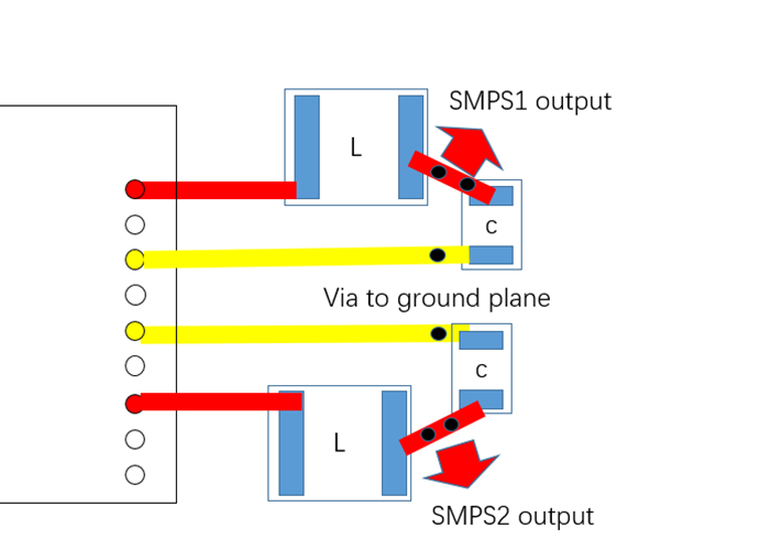
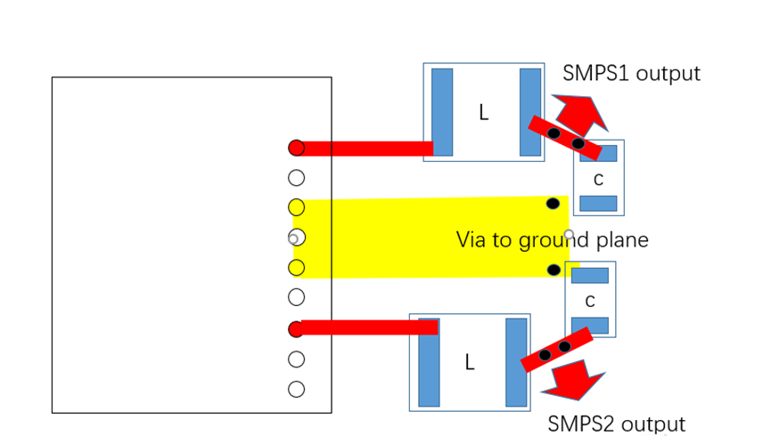
- Implement Dedicated Ground Returns: A critical lesson learned from projects is to avoid a single, large ground pour for multiple SMPS circuits. Instead, use dedicated, independent ground traces for each SMPS output from a PMIC. Since each SMPS may operate at a different switching frequency, connecting their grounds haphazardly can cause cross-talk and interference. Isolated ground paths ensure each channel maintains a minimal and clean current loop, which is vital for stability.
- Below the first picture is correct layout: independent ground traces; The second picture is incorrect layout: shared ground pour.
2. Strategic Component Placement for Minimal Loops
Component placement is the foundation of a good layout. Follow a priority-based approach:
- Prioritize the High-Frequency Switching Loop: This loop, which includes the input capacitor, the power switch (inside the PMIC), and the inductor, is the most critical. Place these three components as close together as physically possible to minimize the loop area. This is the single most effective way to reduce EMI.
- Secure the Output Capacitor Ground: The ground terminal of the output capacitor must have a direct and low-impedance path to the main ground reference. Use a short trace to a dedicated via that connects directly to the main ground plane. Avoid daisy-chaining this ground connection through other circuits, as this can introduce noise and instability.
3. Implement a Careful Grounding Strategy
While a continuous ground plane is beneficial, its implementation around SMPS circuits requires care. The guidance from point #1 takes precedence: the individual SMPS grounds should be kept separate until they are connected at a single-point “star” ground. This strategy prevents noise from one SMPS channel from coupling into another via the common ground plane.
4. Effective Bypassing and Decoupling
High-frequency noise on the supply pins of the control IC (e.g., TL494, IR2153) can cause erratic operation. Place high-quality, low-ESR decoupling capacitors as close as possible to the IC’s power pins. This provides a local, clean energy source for the high-speed switching activity, preventing noise from spreading through the power distribution network.
5. Plan for Thermal Management
Power semiconductor devices like MOSFETs and diodes generate heat. Ensure they have sufficient copper area (often called a “thermal pad” or “pour”) connected to their pins to act as a heat sink. For higher-power designs, use an array of thermal vias under the device to transfer heat to internal ground planes or a dedicated heatsink layer.
For a comprehensive deep dive, consulting a professional Power supply PCB design Guidelines pdf is always recommended, as these resources consolidate years of practical experience.
How Is the SMPS PCB Layout?
The SMPS PCB layout is the core of a successful design. Think of it as the power supply’s “road system.” The layout determines if current and signals “travel” smoothly, without traffic jams or accidents. A superior layout maximizes circuit performance. Here are some core SMPS PCB layout guidelines:
- Separate Critical Paths: Divide the circuit into the power path and the control path. The power path (high-frequency, high-current) should be short and wide. This reduces parasitic inductance and resistance. The control path (sensitive signals) must be kept away from the power path to prevent noise interference.
- Strategic Component Placement: Position the power switch, output rectifier, and input filter capacitor very close together. This creates the smallest possible switching loop area. It is the single most effective way to reduce electromagnetic radiation.
- Judicious Use of Vias: Be careful when using vias to connect layers. For high-current paths, use multiple vias in parallel. This reduces impedance and aids heat dissipation.
- Feedback Path Care: The voltage feedback network must be routed away from noise sources (like inductors and switch nodes). Keep its traces short and direct to avoid picking up noise that causes output instability.
These fundamental principles apply whether it’s a simple 12V power supply PCB layout design or a complex multi-output power distribution PCB. A good layout results from careful planning and iterative optimization.
What Are the Benefits of Using an SMPS?
Opting for SMPS technology, especially on a well-designed SMPS PCB, offers significant advantages:
- High Efficiency: This is the biggest benefit. Efficiencies often exceed 80%, far above the 30-60% of linear supplies. This means less energy is wasted as heat, saving power and cost.
- Compact and Lightweight: High-frequency switching allows for the use of smaller, lighter magnetic components (inductors and transformers). This makes SMPS PCB boards ideal for space-constrained devices.
- Wide Input Voltage Range: SMPS can handle a wide range of fluctuating input voltages while still providing a stable output.
- Flexible Outputs: You can design supplies that provide multiple different output voltages. This meets the needs of complex systems.
Of course, SMPS also has challenges, mainly EMI and design complexity. But this is precisely where the value of an experienced manufacturer shines.
What Is the SMPS PCB Board Price?
This is a very practical question, but the answer is not fixed. The SMPS PCB board price depends on several factors. Understanding them helps with budget planning:
- Layer Count and Complexity: A simple 2-layer board is much cheaper than a multi-layer board requiring precise impedance control.
- Material Requirements: Standard FR-4 material is the most economical. High-power or high-frequency applications may need more expensive materials.
- Board Size: The size directly impacts raw material cost.
- Process Requirements: Copper weight, surface finish (like ENIG or HASL), and other specs affect the price.
- Order Quantity: Volume production typically significantly reduces the unit price.
For instance, a basic 12V SMPS PCB prototype will have a higher price than a mass-produced unit. The SMPS PCB price in India may differ from one manufactured in China, due to local supply chains and costs. The best approach is to request quotes from several suppliers with your specific requirements.
Case of Manufacturing SMPS PCB Board at EBest Circuit (Best Technology)
When a leading industrial automation manufacturer approached us with a critical power supply challenge, their requirements pushed conventional manufacturing limits. The application: a next-generation sensor network node requiring a 24V SMPS power supply PCB that could deliver 96% efficiency while fitting into an unprecedented compact form factor. The constraints were severe: 45mm x 60mm board dimensions with mandatory compliance to industrial EMC standards (IEC 61000-4-2 Level 3).
The technical challenges were immediately apparent:
- Power density requirements exceeding 2W/cm³
- Radiated emissions margins needing 6dB below Class A limits
- Operating temperature range of -40°C to +105°C ambient
- 100,000-hour MTBF requirement with derating to 60% of component ratings
Our engineering team initiated a comprehensive design-for-manufacturing analysis that revealed critical optimizations. By re-architecting the component placement to create a unified thermal management zone, we reduced the switching loop area by 42% compared to the client’s initial layout. We implemented a 6-layer sequential lamination stackup with 3OZ finished copper weight on critical power layers, using Isola 370HR high-Tg material for enhanced thermal reliability.
Manufacturing execution leveraged our specialized capabilities:
- Precision imaging: 75μm laser-drilled microvias enabling high-density interconnects
- Advanced plating: 25μm copper filling on through-vias for enhanced current carrying capacity
- Thermal management: Embedded copper coins beneath the power MOSFETs, achieving 18°C lower junction temperatures
- EMI control: Shielded inductor cavities with selective gold plating on contact surfaces
This success was built upon our specialized SMPS manufacturing capabilities:
- High-density interconnects with 40μm line width/spacing tolerance
- 2-20 layer constructions with 20OZ maximum copper thickness
- 0.2mm mechanical laser via drilling capability
- Mixed material bonding (FR-4, Rogers, polyimide) for thermal management
- 100% electrical testing with 4-wire Kelvin measurement for power integrity
- 3D X-ray inspection for hidden solder joint and via integrity
Why Should You Choose EBest Circuit (Best Technology) as Your Reliable SMPS PCB Assembly Supplier?
With many options available, why is EBest Circuit (Best Technology) your ideal partner for SMPS PCB assembly?
- Deep Technical Expertise: We don’t just make boards; we understand power electronics. Our engineering team is well-versed in SMPS PCB design guidelines. We can provide valuable feedback before manufacturing even begins.
- Advanced Manufacturing Capability: We possess the advanced equipment needed to produce high-reliability, multi-layer SMPS PCBs. We ensure every board meets specifications.
- Stringent Quality Control: We implement a rigorous quality management system from incoming materials to final testing. We know how critical power integrity is to the end product.
- Comprehensive Service: We offer a full turnkey service, from SMPS PCB fabrication to component sourcing and assembly. This saves you time and effort.
- Competitive Pricing: Through optimized processes and mature supply chain management, we deliver great value, helping you control costs.
Whether you need to evaluate the SMPS PCB board price, require an SMPS PCB manual for reference, or are looking for a custom solution like a Worcester SMPS PCB conversion kit, we are ready to support you.
In summary, the SMPS PCB is the core of modern electronics. It turns efficient switching power technology into stable, reliable reality. We hope this article gave you a clearer understanding of its design, application, and value.
At EBest Circuit (Best Technology), we specialize in SMPS PCB design, SMPS power supply PCB layout, high-quality SMPS PCB fabrication, and wholesale SMPS PCB assembly. If you are looking for a trusted SMPS PCB supplier for your next project, please send your requirements and related files like SMPS circuit diagram PDF to sales@bestpcbs.com. Our expert team is ready to provide professional technical and pricing consultation.
You may also like


Tags: SMPS PCB