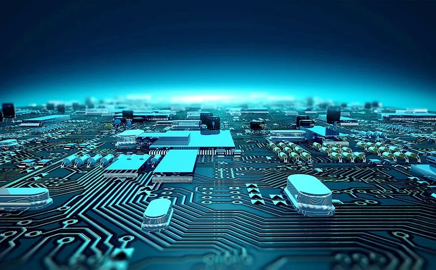
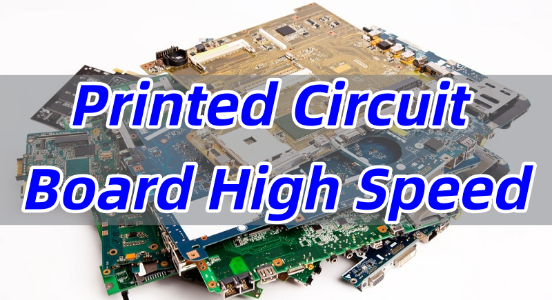
Printed circuit board high speed design is at the heart of today’s advanced electronics. The blog presents points about meaning, features, material, design, manufacturing process, applications of high speed PCB board, and where to get best printed circuit board high speed.
Have you encountered these challenges in your experience?
- The tricky problem of signal integrity?
- The increasing complexity for design and the increasing cost?
- Increasing difficulty of manufacture and inspection?
- Unstable performance and reliability problem?
To resolve the difficulties presented, kindly consider the following methods.
- Optimize the design and layout: For example, boost PCB stacked structure, layout, and impedance control to elevate signal completeness.
- Adopt cutting-edge manufacturing process: Use high precision manufacturing process, such as micro via design, back-drilling technology, in order to decrease signal loss and reflection.
- Present tailored ideal solutions: To meet different needs in application via giving a customizable design according to customer demands, such as high-frequency signal processing, high speed interface design, high-frequency inspection, etc.
- Offer technical support and inspection service: Present signal completeness analysis, impedance test, high frequency inspection, and other services, aiming to help customers to verify design and enhance performance.
As a PCB high speed manufacturer in China, EBest Circuit (Best Technology) is aiming to provide good quality printed circuit board high speed, and give proper solutions for high frequency signal optimization, impedance control, and EMI reduction to meet the demanding requirements of modern electronic systems. You’ll find these products in our lineup: high speed PCB, HDI PCB, high frequency PCB, and others. If you require high speed design PCB for the 5G communication, data center, high speed interface, or other high speed communication occasions, pls write an email to us for the BEST support at sales@bestpcbs.com.
What is printed circuit board high speed?
A high-speed printed circuit board (PCB) refers to a board used in circuits where signals change extremely rapidly, not just a PCB with a high operating frequency. When the signal switching is so fast that transmission line effects can no longer be ignored, the PCB is classified as high-speed. Here, “switching” specifically refers to the signal rise and fall edges.
What Is Transmission Line Effect?
One key aspect of high-speed PCB design is the transmission line effect:
- Ordinary PCB: Traces are treated as simple connections, and designers generally do not need to consider delay, reflections, or impedance issues.
- High-speed PCB: Traces act as transmission lines. Designers must carefully account for impedance matching, signal propagation delay, and electromagnetic compatibility (EMC). Improper design can cause signal distortion or timing errors.
What Are Signal Rise and Fall Edges?
To understand high-speed PCBs, it is important to know what rise and fall edges mean:
- Rise edge: The transition of a signal from a low level to a high level.
- Fall edge: The transition of a signal from a high level back to a low level.
These edges define how quickly a signal switches between voltage states, and their speed directly impacts the design requirements of the PCB.
Low and High Logic Levels
It is particularly important to know that digital circuits operate between two voltage states:
- Low level (logic 0): Usually close to the ground potential, representing the “off” state.
- High level (logic 1): At a higher voltage (for example, 3.3V or 5V), representing the “on” state.
The challenge in high-speed PCBs arises when signals switch very rapidly between low and high levels. The faster the rise and fall edges, the more the circuit behaves like it is operating in a high-frequency environment, which places stricter demands on layout and signal integrity.
Difference Between High-Frequency PCB and High-Speed PCB
The terms high-frequency and high-speed PCBs are often grouped together as “high-frequency high-speed PCBs”, but they have different focuses:
- High-frequency PCB: Applied in RF and microwave circuits, operating above 300 MHz and often into the GHz range. Material requirements are strict, including dielectric constant (DK) and dissipation factor (DF). Common materials include PTFE. The design emphasis is on impedance control.
- High-speed PCB: Applied in high-speed digital circuits. Even if the clock frequency is not extremely high, if the signal’s rise and fall edges are very fast, the board must be designed as high-speed. The design emphasis is on delay matching and signal integrity.
In summary, the distinction between high-frequency boards and high-speed boards is primarily based on application rather than material selection.
What are the features of high-speed signals in PCB?
1. Common High-Speed Interfaces
The most direct way to identify whether a PCB is high-speed is by checking the interfaces it supports.
- High-speed: DDR4 memory (2400MT/s), PCIe 4.0 (16Gbps), USB 3.1 (10Gbps), HDMI 2.0 (18Gbps). These run at extremely fast speeds, with signal edges switching within a few hundred picoseconds.
👉 Example: DDR4 data lines toggle more than 10,000 times faster than a standard UART line. - Low-speed: UART (115.2kbps), I2C (400kHz), CAN bus (1Mbps). These protocols are much slower and do not impose strict PCB design requirements.
2. Clock Frequency and Data Rate
- High-speed: Frequencies usually exceed 100MHz and data rates reach 1–10Gbps or more. For instance, PCIe 3.0 runs at 8Gbps per lane.
- Low-speed: Frequencies typically stay below 50MHz with data rates in the kbps–Mbps range.
📖 Clock frequency = the number of signal cycles per second. Higher frequency means faster transitions, which makes the design more challenging.
3. Rise Time and Fall Time
The edge of a signal refers to the transition between low and high states.
- High-speed: When rise/fall time is shorter than 500ps (0.5ns), the circuit must be treated as high-speed.
👉 Example: A 10cm PCB trace has ~0.6ns delay. If the signal edge is only 300ps, reflections will occur and special design rules are required. - Low-speed: Rise/fall times above 1–10ns. Even with longer traces, signal distortion is minimal.
📖 Reflection = part of the signal bounces back along the trace, like an echo, which can distort data.
4. Signal Propagation Speed
Signals in a PCB do not move at light speed. They typically travel at ~60% the speed of light, which is ~15cm/ns in FR4 material.
- High-speed: A 30cm trace introduces ~2ns delay, which must be compensated in timing-sensitive designs like DDR.
- Low-speed: If the signal period is much longer (tens of ns), this delay is negligible.
📖 FR4 = a common fiberglass epoxy board material, cost-effective but lossy at high frequencies.
5. Power Integrity Requirements
- High-speed: Power supply must remain very stable. For DDR4 at 1.2V, even ±60mV noise may cause errors. Decoupling capacitors and solid power planes are required.
- Low-speed: A 5V microcontroller may tolerate 5.2V supply without affecting UART signals.
📖 Decoupling capacitors = small capacitors placed near chips to absorb power noise and stabilize voltage.
6. Impedance Control and Reflections
- High-speed: Controlled impedance is mandatory. USB 3.0 requires 90Ω differential impedance, HDMI needs 100Ω. Any deviation above ±10% causes reflections and data loss.
👉 Engineers use an eye diagram to measure quality. If the “eye” shape closes, the signal is unreadable. - Low-speed: Impedance variations have little effect; signals remain stable even without strict control.
📖 Differential impedance = the combined resistance seen by two complementary signals traveling together.
7. Crosstalk and EMI
- High-speed: Closely spaced traces can interfere (crosstalk). For DDR, traces must be spaced at least three times their width. High-speed signals also radiate electromagnetic energy, causing EMI. Shielding and ground planes are essential.
- Low-speed: Slower signals rarely affect nearby traces and produce little EMI.
📖 EMI (Electromagnetic Interference) = unwanted radiation from circuits that can disturb nearby devices.
8. Material and Process Sensitivity
- High-speed: Advanced laminates like Rogers RO4350B (Dk=3.48, Df=0.0037) are often used. They minimize loss and distortion at multi-gigabit rates.
👉 Example: Using standard FR4 (Dk≈4.5, Df≈0.02) at 10Gbps results in severe waveform distortion and eye diagram closure. - Low-speed: FR4 is sufficient for microcontrollers, sensors, and control circuits with modest speeds.
📖 Dielectric constant (Dk) = how much slower signals travel in a material compared to vacuum. Loss factor (Df) = how much energy the signal loses as heat.
To conclude, high-speed PCBs are defined not just by frequency, but by how fast signals switch, how quickly they propagate, and how sensitive they are to layout, materials, and power supply. Key indicators include signal interfaces like DDR, PCIe, USB, and HDMI, clock frequencies above 100MHz, data rates in Gbps, and rise/fall times below 500ps. Compared with low-speed boards, high-speed designs require strict impedance control, careful trace spacing to reduce crosstalk, stable power distribution, and advanced low-loss materials to maintain signal integrity. Understanding these features helps engineers predict potential problems early and ensure reliable, high-performance circuits.
📖 In short: if your board has ultra-fast signals, tight timing requirements, and sensitive high-speed interfaces, treat it as a high-speed PCB and apply the proper design practices.
What are high speed PCB materials?
High-speed PCBs are used in circuits with high-frequency signals and fast data transmission, such as communication base stations, automotive systems, satellite communications, and military radar. Choosing the right material is crucial for signal integrity and low signal loss. Common high-speed PCB materials include Hydrocarbon Resin, PTFE, LCP (Liquid Crystal Polymer), and PPE/PPO.
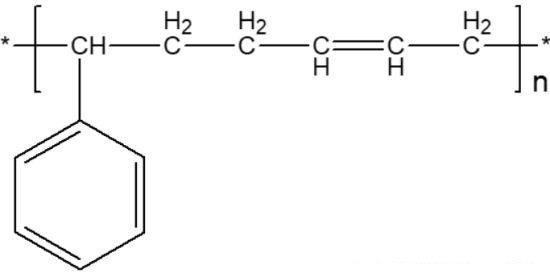
1. Hydrocarbon Resin
Hydrocarbon resins are polymers composed of carbon and hydrogen, including styrene-butadiene copolymer, polystyrene, and styrene-divinylbenzene copolymer.
Key properties:
- Excellent dielectric properties: Dk ≈ 2.4, Df ≈ 0.0002
- High thermal resistance
- Good chemical resistance
Applications: Suitable for microwave circuits and high-frequency communication modules.
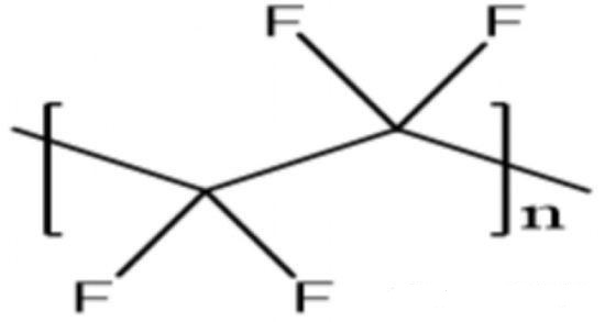
2. PTFE Flexible Film
PTFE is a fluoropolymer with low dielectric constant and low signal loss, ideal for high-speed, high-frequency signals.
Processing methods: Molding, impregnation, extrusion, etc.
Modified PTFE: Enhanced with ceramic or glass fiber to improve mechanical strength and stability.
Applications: Used in millimeter-wave communication, 5G PCBs, satellite antennas, and radar modules.
Notes:
- Millimeter-wave: Electromagnetic waves with frequencies from 30–300 GHz and wavelengths 1–10 mm.
3. LCP (Liquid Crystal Polymer)
LCP is a high-performance plastic combining liquid flow and crystalline molecular order, forming a “liquid crystal state”.
Properties:
- Can flow when melted or dissolved but retains ordered molecular structure (anisotropic properties).
- Three main types: multi-phenyl copolymers, naphthalene-containing, aliphatic chain segments.
- Thermal resistance varies by type: Type I > Type II > Type III
Applications: High-speed interfaces (HDMI, USB 3.1, PCIe), antenna modules, and microwave circuits.
Notes:
- Anisotropy: Material properties differ along different directions.
- Liquid crystal state: Intermediate state between solid and liquid with ordered molecular alignment.
4. PPE/PPO (Polyphenylene Ether / Oxide)
PPE/PPO is a high-strength engineering plastic with rigid aromatic chains and methyl groups blocking reactive sites, providing high rigidity, thermal stability, and chemical resistance.
Properties:
- Ether bonds add flexibility but reduce thermal resistance.
- Hydrophobic, low water absorption, excellent dimensional stability, and insulation.
- High viscosity; more difficult to process.
Applications: Used in high-speed PCBs requiring good insulation and stability, e.g., aerospace electronics and high-speed communication devices.
Notes:
- Dimensional stability: Material size changes little with temperature or humidity.
- Insulation: Prevents unwanted current flow, protecting signal quality.
Summary of Material Selection
High-speed PCB materials differ from standard FR4 boards in having:
- Low dielectric constant (faster signal, lower loss)
- Low loss (reduced signal attenuation)
- High thermal stability
- Good mechanical strength
They are widely applied in communication base stations (antennas, amplifiers, filters), automotive systems, satellite communications, satellite TV, military radar, and high-frequency communication devices. Material selection significantly impacts signal integrity, reflection, interference, and transmission loss, making it a critical factor in high-speed PCB design.
| Material | Dielectric Constant (Dk) | Loss Tangent (Df) | Typical Frequency Range |
|---|---|---|---|
| Hydrocarbon Resin | 2.4 | 0.0002 | Up to ~10 GHz |
| PTFE | 2.0–2.1 | 0.0009 | Up to ~50 GHz |
| LCP | 2.9–3.0 | 0.002 | Up to ~40 GHz |
| PPE/PPO | 2.6–2.8 | 0.002–0.003 | Up to ~20 GHz |
Table Notes
- Dielectric Constant (Dk): Lower Dk allows faster signal propagation.
- Loss Tangent (Df): Lower Df means less signal energy is lost during transmission.
- Thermal Resistance: Lower value is better; material can conduct heat efficiently, keeping components cooler.
- Processing Difficulty: Relative ranking of manufacturing complexity, including cutting, lamination, drilling, and copper plating.
High-speed PCB design guidelines
Before designing a PCB, it is essential to understand the difference between high-speed and low-speed PCBs.
Signal Frequency and Speed
- Low-speed PCBs handle signals below tens of MHz, where trace length and impedance have little impact. Design mainly focuses on circuit functionality and reliability, with minimal EMI concerns. Typical uses include simple control boards and sensor interfaces.
- High-speed PCBs operate from 100 MHz to several GHz, with fast rise/fall times. Signal integrity depends on trace length, routing, impedance, and stack-up. Applications include high-speed interfaces, 5G modules, and data acquisition, where precise signal control is critical.
Design Complexity
- Low-speed PCB design is simple, with minimal EMI or crosstalk concerns. Focus is on power distribution, compact layout, and basic decoupling. Fewer layers and shorter design cycles are typical.
- High-speed PCB design is complex. Signal integrity, power integrity, impedance control, differential pairs, multilayer stack-ups, and continuous ground planes are critical. Routing and placement directly affect performance, requiring simulation and strict design rules.
Here is the high-speed PCB design guidelines for your review.
1. Layout Planning
- Shorten critical signal paths and avoid loops to reduce interference. Place clocks and high-speed traces first, keeping sensitive analog or low-frequency circuits separate. Keep high-speed traces near continuous ground planes, and avoid sharp turns or unnecessary zigzags to minimize reflection and crosstalk.
2. Impedance Control
- Maintain consistent trace impedance for high-speed signals. Use microstrip or stripline structures depending on board layers, and calculate trace width, spacing, and dielectric thickness to meet target impedance.
Common Impedance Models:
- 50Ω single-ended: Widely used in RF and high-speed digital signals; matches common connectors, PCB traces, and IC I/O impedance.
- 90–100Ω differential: Used for USB, HDMI, Ethernet, and other high-speed differential signals; ensures differential consistency and reduces common-mode noise.
Avoid vias on critical paths and verify impedance continuity with design or simulation tools.
3. Ground Plane Design
- Use a continuous ground plane to reduce noise and improve EMI performance. Ensure critical signal return paths follow the shortest route along uninterrupted ground. Keep power and ground planes close, and place decoupling capacitors near high-speed device power pins.
4. Component Selection
- Use low-ESR capacitors for high-speed signals and avoid high-inductance components on critical paths. Choose high-frequency connectors for interfaces like USB3.0, PCIe, or HDMI. For GHz-level signals, consider low-loss materials (e.g., Rogers) to reduce signal attenuation.
5. Advanced Techniques
- Microstrip vs. Stripline: Use stripline for critical high-speed signals for better shielding; microstrip can be used where layout flexibility is needed.
- Differential Pairs: Maintain even spacing and matched lengths (within ~20 mils, 0.5 mm). Keep traces near ground planes and avoid excessive vias or splits.
- Simulation: Use EDA tools (Altium, Cadence, HyperLynx) to check signal integrity, power integrity, crosstalk, and timing. Adjust trace length, impedance, differential pair layout, and decoupling based on simulation results.
Why use more copper in high speed PCB?
In high-speed PCB design, the amount and distribution of copper directly affect signal integrity, thermal performance, and electromagnetic compatibility (EMC). Key reasons for increasing copper usage include:
1. Improve Signal Integrity
- Reduce impedance discontinuities: High-speed signals are sensitive to impedance changes. Thicker copper or additional copper pours help minimize transmission line impedance variations, preventing signal reflection.
- Optimize return paths: A continuous ground plane (e.g., GND layer) provides low-impedance return paths for high-frequency signals, reducing crosstalk and noise.
2. Enhance Thermal Performance
- High thermal conductivity: Copper’s thermal conductivity (~380 W/m·K) far exceeds FR4 (0.2–0.3 W/m·K), quickly dissipating chip heat and preventing performance degradation due to temperature rise.
- Thermal stability: Copper substrates maintain dimensional stability under high temperatures (e.g., server CPUs), reducing thermal deformation effects on signal quality.
3. Improve Electromagnetic Compatibility (EMC)
- Shielding: Large copper pours (e.g., PGND) help shield external EMI and suppress internal signal radiation.
- Reduce eddy current loss: High-frequency signals can induce circulating currents (eddy currents) in conductive planes. Proper copper distribution reduces these currents, minimizing energy loss and signal attenuation.
4. Support High-Density Routing
- Multilayer stack-ups: High-speed PCBs often have 8 layers or more. Copper layers are used for power and ground planes, ensuring power integrity and signal isolation.
- Plated through-holes (PTH): Copper in vias ensures reliable inter-layer connections with low resistance and minimal parasitic inductance.
5. Material and Process Considerations
- High-frequency substrate integration: When combining Rogers and FR4, copper layers must match the low-loss characteristics of high-frequency materials (Df < 0.004).
- Cost-performance balance: Full-copper substrates are expensive, but critical signal layers (e.g., RF channels) require copper to ensure performance.
In summary, increasing copper usage in high-speed PCBs is driven by signal integrity, thermal management, and EMC requirements. Optimizing copper thickness, copper pours, and stack-up design is essential for applications such as 5G and AI chips.
What are the applications of high speed PCB?
High-speed PCBs are specially designed circuit boards for high-speed signal transmission. They feature excellent high-frequency performance, low-noise characteristics, high-density capability, and superior overall performance. These boards are widely used across various industries.
1. Communication
High-speed PCBs are widely used in communication systems, including mobile networks, satellite communication, and optical communication. They enable fast signal transmission and processing, improving system performance and reliability.
2. Printed Circuit Boards for High Speed Computing
In the computing field, high-speed PCBs are essential for servers, storage devices, graphics cards, and other high-performance computing equipment. They ensure rapid signal transfer and processing, enhancing overall system efficiency and reliability.
3. Consumer Electronics
High-speed PCBs are commonly found in consumer electronics such as smartphones, tablets, and digital cameras. They support fast signal transmission and processing, boosting product performance and user experience.
4. Automotive Electronics
High-speed PCBs are applied in automotive systems, including engine control units, body control modules, and in-car entertainment systems. They provide reliable high-speed signal processing, enhancing automotive system performance.
5. Industrial Control
High-speed PCBs are used in industrial automation, robotics, and intelligent instrumentation. They enable fast and accurate signal processing, improving the efficiency and reliability of industrial control systems.
Each of these applications requires boards that manage both frequency and signal clarity without failure.
Where to get Best printed circuit board high speed?
Finding the Best printed circuit board high speed solution means choosing a supplier who understands material science, signal behavior, and precision manufacturing. Many companies face pain points like extended lead times, inconsistent quality, or lack of design support. At EBest Circuit (Best Technology), we solve these challenges with:
- Quality Assurance: ISO 9001, ISO 13485, IATF 16949, and AS9100D certifications for strict quality assurance.
- Technical Guidance: Professional technical support to review layouts and suggest improvements.
- Cutting-edge Machine: Equipped with sophisticated equipment for high precision prototyping, manufacturing, and assembling different-layer printed circuit board high speed, such as 4 layer high speed PCB, 6 layer PCB stackup for high speed, and others.
- Integrated Factory: Own original PCB and SMT factory to expedite the lead time more efficiently, saving communication costs and time.
- Good Quality Supply Chain: Maintain a stable supply chain through partnerships with Tier 1 material suppliers like Rogers and Isola, ensuring continuous availability of high-frequency laminates, copper foils, and prepregs. Buffer stocks of critical components support rapid turnaround for high-speed PCB production.
With strong supply chain control and advanced machines, we deliver reliable high-speed PCBs that meet global standards. Customers gain not only a product but a trusted partner for long-term cooperation.
In a nutshell, printed circuit board high speed is very critical for the high-frequency signal integrity and electromagnetic compatibility in advanced electronics applications, where even minor impedance mismatches can lead to data corruption or system failures. So understanding its definition, characteristics, applications, selecting the right materials, and mastering the full knowledge of design will significantly enhance your project efficiency and ensure optimal performance in demanding electronic systems. If there’s any new inquiry, pls let us know via sales@bestpcbs.com. We will make our full engagement to give a satisfactory solution for you.