

PCB copper pad quality is crucial for any printed circuit board to perform well in the field. In this blog, we mainly explains what PCB copper pads are, their types, surface finishes, functions, common peeling issues, and practical repair and material selection solutions for reliable manufacturing.
Have you experienced these nightmares and headaches in your project?
- The mechanical damage and the mechanical stress issues?
- The material and process problem caused the pad peeling?
- Poor soldering and thermal stress?
- The defect of the design and manufacturing?
Here are the solutions and the measures that EBest Circuit (Best Technology) recommends.
- Optimize the soldering process: control the soldering temperature and time according to the types of PCB pads; use the premium quality soldering irons and solder.
- Improve the material and the process: Boost copper coil quality to ensure sufficient adhesion between the copper and the resin. Besides, it is vital to improve the manufacturing process, such as lamination, etching, and plating, to ensure strong bonding between the copper foil and the substrate.
- Optimize design and the storage condition: First, we should increase the distance between the copper foil and the edge to reduce the mechanical stress and avoid being too near between the copper foil and the edge. Second, the point is to avoid exposure to the moist environment for a long time.
- Boost the thermal stability of the pads: We will increase the copper foil thickness via plating or other ways to boost the thermal conductivity and reduce the localized high temperatures impact to the pads. Finally, using the better quality copper foil guarantees great adhesion between the copper and the resin.
EBest Circuit (Best Technology) provides various PCB types to a much larger market for over 19 years, such as bus bar PCB, RF board, HDI PCB, High Tg PCB, extra thin PCB, and others. We have a rigorous quality inspection system, where each manufacturing process will undergo strict QC. If you require PCBs, just feel free to write an email to sales@bestpcbs.com or make a call at +86-755-2909-1601.
What is a PCB Copper Pad?
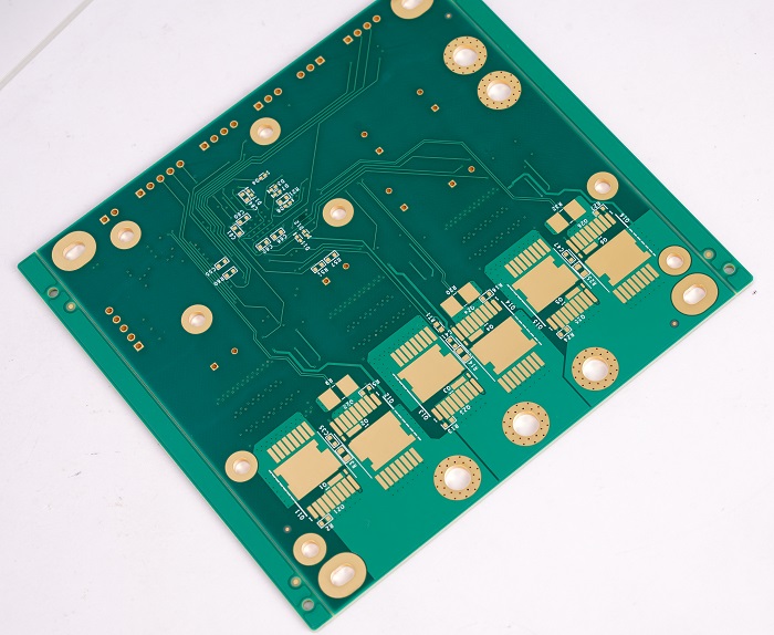
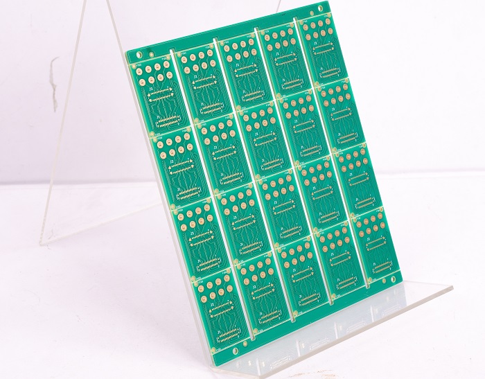
A PCB copper pad is the conductive surface on a printed circuit board where components are soldered or connected. These pads provide electrical and mechanical connections between the board and electronic parts. It is nice to know to know that the shape of the pad can be round, square, or a tailored shape. That is beneficial to meet the design demands. The exceptional quality pads ensure stable soldering, low signal loss, and long-term stability.
In our experience at EBest Circuit (Best Technology), many customers approach us after facing poor pad adhesion from other suppliers. We avoid these problems before shipping via using outstanding quality copper foil, high precision etching, and strict quality inspection.
What Are the Different Types of PCB Pads?
It is helpful to know that the PCB pads include the following types.
- Through-Hole Pads: It is a drilling hole with the plated copper, used for the component leads to pass through and solder. That provides the mechanical support.
- SMD Pads: It is used in the flat copper area of the surface-mounted components, suitable for high-density circuit boards.
- Thermal Relief Pads: It is designed for controlling the heat flux during soldering to avoid overheating.
- Via Pads: Connect the inner layers of multi-layer boards, generally smaller than component pads and critical to multi-layer boards.
It is really significant to select the suitable types of pads, since it will affect the assembly speed, soldering strength, and the performance of the integrated boards.
SMD Pads PCB vs Through-Hole Pads: Which is Better for Your PCB?
SMD pads PCB designs are preferred in high-density and lightweight applications like smartphones and wearable devices. They allow smaller boards and faster automated assembly.
Through-hole pads is a good fit for the components that needs extra mechanical strength, such as connectors or high-power device. It is commonly to see that the through-hole pads are used in places where stability is needed and the SMD pads are used in high density areas. In many projects, engineers will prefer to use the hybrid designs.
What is a PCB Copper Pad Surface Finish?
Surface finish is the coating applied to the copper pad to protect it from oxidation and ensure good solderability. The common surface treatments include HASL, ENIG, OSP, immersion Tin, immersion silver, and hard gold plating. For PCB copper pad, it is mostly used ENIG for its smooth surface, oxidation resistance, and long lifespan.
EBest Circuit (Best Technology) uses ENIG or hard gold plating for the applications that require high reliability, such as aerospace, to ensure the high-quality soldering performance even after months of storage.
What is the Function of the PCB Cu Pad?
PCB Cu pad is not only an electrical connection point but also a mechanical fix point of the components. It keeps the signal transmission efficiency and maintains the stable performance of the components in the situation of vibration or mechanical stress. It is great to know that no reliable pad, even the most advanced circuit design, can fail.
Why Do PCB Copper Pad Peels?
It is valuable to know why the PCB copper pad peels.
- One common reason is poor adhesion between the copper and the substrate. This can happen if there is not enough lamination pressure or if the surface is contaminated.
- The second crucial point is that the excessive heat of the soldering will cut the bond strength.
- The third essential reason is that the mechanical stress is too high in the assembly or the repairing process, which pull pads away from the laminate.
It is known that the PCB copper pad peels will increase the rework difficulty and the costs. EBest Circuit (Best Technology) prevents these issues through controlling the process temperature, using professional quality substrates, and making the peel strength test meanwhile.
3 Fixes for PCB Copper Pad Peels in Manufacturing
Based on industry experience, here are three effective solutions:
- Improve Lamination Process: Ensure clean substrate surfaces and use proper lamination pressure to achieve strong copper adhesion.
- Control the Soldering Temperature: Make use of the preheat process to protect the pads from overheating.
- Improve the material quality: Choose the high-strength copper and the outstanding quality substrate to reduce the risk of PCB copper pad peels.
The customer complaints are significantly reduced when EBest Circuit (Best Technology) applies these measures. We have received the repeat orders and the good project results.
How to Do PCB Copper Pad Repair for PCB Factory?
There are several steps to repair the PCB copper pad for peeling.
- The first step is to clean the damaged areas.
- The second crucial step is to apply the suitable adhesives or epoxy.
- The third critical point is to employ the copper foil cut precisely or the compatible pads, instead of using the original pads.
- The final point is to make sure that the repaired pads are compatible with the mechanical and electrical standards.
The process can be simplified by using the PCB pad repair kit. EBest Circuit (Best Technology) matches the original pad size strictly and the surface treatment during the repair process. It aims to guarantee that the reliability of the repaired boards is the same as the original boards.
How to Choose the Right PCB Pad Material for Your Project?
Pad material choice affects conductivity, solderability, and long-term performance. For most commercial boards, copper is the standard due to its high conductivity. The plating or coating material—gold, tin, silver—should match your assembly method and storage conditions. For example, ENIG is ideal for fine-pitch SMD pads PCB designs, while HASL may suit cost-sensitive projects.
EBest Circuit (Best Technology) helps customers evaluate these factors to reduce rework rates and extend product lifespan. If you have any further questions, pls contact us at +86-755-2909-1601 or sales@bestpcbs.com.
All in all, the reliability of the PCB copper pad takes center stage in manufacturing. Every process is related to the circuit board quality, from the types of PCB pads, surface treatment, and the measures to tackle the problem of peeling. The manufacturer can improve the issue of pad peeling via proper material selection, strict process control, and viable maintenance methods. EBest Circuit (Best Technology) is 100 percent dedicated to solving the pain point of pad peeling and the rework. With our qualified manufacturing process as per the ISO standard, professional engineers, and the customers’ first service, we are excelling in providing good quality PCBs to the market. If you need to order PCBs or PCBA, just let us know at sales@bestpcbs.com.
Tags: PCB Copper Pad