

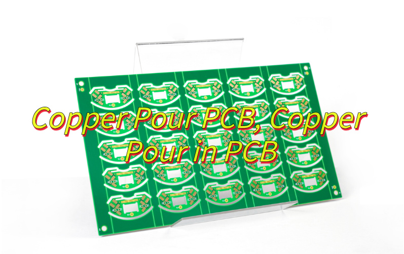
What is copper pour PCB? Let’s discover its function, application, clearance design rules, grounding and connection problems and solutions, dead zones and sharp problems and solutions.
Are you worried about these problems?
- Why does my high-speed PCB always have signal integrity issues?
- How can I reduce thermal hotspots in dense component layouts?
- What’s the most cost-effective way to improve EMI performance?
EBest Circuit (Best Technology) can provide service and solutions:
- Optimized copper pour design: Reduces impedance discontinuities and crosstalk by providing uniform current paths.)
- Thermal-balanced copper pour: Dissipates heat evenly through enhanced thermal conductivity.)
- EMI-shielded copper pour: Acts as a natural Faraday cage to minimize radiated emissions.)
Welcome to contact us if you have any request for copper pour PCB: sales@bestpcbs.com.
What is Copper Pour PCB?
Copper pour PCB (also called as copper pour in PCB) design refers to the technique of filling unused areas on a circuit board with conductive copper, typically connected to ground or power networks. It involves filling blank areas of a circuit board (not layout traces) with a continuous layer of copper foil using polygonal fills automatically generated by the design software. These copper foil areas are typically connected to the board’s ground plane (GND) or power plane (VCC), forming a complete conductive layer.
What is the Purpose of the Copper Pour on a PCB?
- Signal Integrity: Provides low-impedance return paths for high-frequency signals, reducing electromagnetic loss.
- EMI/RFI Shielding: Acts as conductive shielding to suppress external/internal electromagnetic interference.
- Thermal Dissipation: Enhances heat transfer from high-power components via copper’s thermal conductivity.
- Power Stability: Stabilizes voltage delivery through low-inductance copper planes for high-current circuits.
- Structural Integrity: Balances copper distribution to prevent board warpage during fabrication.
- Cost Efficiency: Reduces production costs by minimizing copper etching waste and simplifying processes.
- Impedance Matching: Enables precise impedance control for high-speed signals via ground plane integration.
What Are Applications of Copper Pour PCB?
- Lighting Systems: LED streetlights, automotive lights, surgical lighting.
- Automotive Electronics: Electric vehicle battery management, motor controllers, charging systems, and headlight drivers.
- Communications Equipment: 5G/6G base stations, RF amplifiers, antenna modules, and filtering devices.
- Industrial Equipment: Welding machines, solar inverters, UPS power supplies, and robotic control systems.
- Medical Equipment: MRI systems, X-ray machines, and surgical laser equipment.
- Computers and Consumer Electronics: CPU motherboards, game consoles, and smartphones.
- Aerospace: Satellite communications, radar, and avionics equipment.
What is the Difference between Copper Pour and Trace?
| Characteristic | Trace | Copper Pour |
| Definition | Conductive path for signal/current | Filled copper area for functional/thermal purposes |
| Function | Signal/current transmission | Heat dissipation, EMI shielding, high-current carrying |
| Smart Avoidance | None (manual adjustment required) | Auto-isolates from other networks |
| Design Method | Manual routing line by line | Auto-fills irregular regions |
| Short Circuit Risk | Low (independent path) | High for standard pour, low for filled pour |
| High-Frequency Adaptability | Susceptible to interference (requires width/spacing optimization) | Reduces crosstalk (avoids via resonance) |
| Typical Thickness | 0.7 mil (½ oz) or 1.4 mil (1 oz) | 4 mil (standard) |
PCB Copper Pour Clearance Design Rules
1. Core Spacing Values
- General Baseline: Copper pad to pad/via distance ≥0.2mm (1oz copper foil) or ≥0.33mm (2.5oz copper foil). Any distance below this will result in a short circuit.
- High-voltage scenarios: Calculate clearance based on voltage (e.g., 220V requires ≥2.5mm), using the maximum of clearance and creepage distances.
- Board Edge Treatment: Copper pad to cutting line ≥0.8mm; otherwise, the copper sheet may tear during milling.
2. Specific Scenarios
- Under capacitors: Copper pads are strictly prohibited, with a spacing of 0.1mm (to prevent parasitic capacitance from interfering with signals).
- Antenna Area: Clearance below wireless modules ≥12.5mm (to prevent signal coupling, measured values).
- Gold-plated board edges: Copper pad setback ≥0.5mm (to prevent corrosion caused by plating solution infiltration).
3. Software Practice (AD/KiCad)
Rule Settings:
- Global Spacing: Start at 0.5mm (20mil), with separate rules for high-voltage areas.
- Copper Pad Specific: Set to 0.8mm when no solder mask is present (to facilitate repair and soldering).
- Priority Suppression: Board-Level Rules > Net-Level Rules > Single-Object Rules. In case of conflict, the strictest value is used.
4. Manufacturing Minefields
- Peelable Structures: Isolated copper islands in the copper pad with a width less than 0.2mm will be deleted (etching will cause breakage).
- Copper Layer Text: Text must be ≥0.15mm away from the copper pad (otherwise, the silkscreen will be blurred).
- Sharp Angle Prohibition: Copper pad corners must be ≥45° (sharp corners can cause excessive corrosion during acid etching).
5. Signal Terms
- High-Speed Lines: Copper pads must be ≥3 times the line width away from clock lines (e.g., a 0.2mm line width requires a 0.6mm setback).
- Grounding copper: The spacing between copper layers in different voltage domains should be ≥1mm (to prevent leakage current).
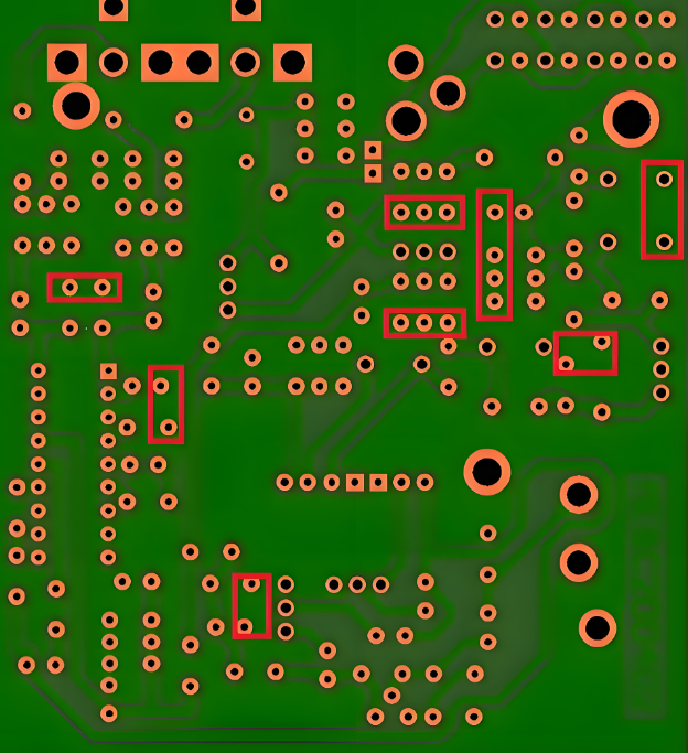
Dead Zones and Sharp Angles Problems in Copper Pour PCB Design
Dead Zone Problems:
1. Electrical Isolation Failure: Isolated copper areas not connected to the network (dead copper) create an antenna effect, increasing electromagnetic interference (EMI), causing high-frequency signal distortion or noise interference.
2. Thermal Stress Concentration: Dead copper cannot effectively dissipate heat, causing local overheating that accelerates component aging and shortens PCB life.
3. Manufacturing Defect Risk: Dead copper can easily peel during etching, causing shorts or opens.
Dead Zone Solutions:
1. Ground Via Connection Design: Add ground vias (vias) in large dead copper areas, connecting them directly to the ground network (recommended density ≥ 1 per square centimeter) to eliminate the antenna effect.
2. Copper Layer Optimization Strategy: Avoid copper pouring in unrouted areas (such as mid-layer routing openings); use a grid-like window design (heat dissipation vias) to improve heat dissipation.
3. Automated Design for Factoring (DFM) Checking: Use EDA tools to run DFM rule checks (e.g., Gerber files with board outlines) to automatically identify and remove dead copper areas.
Sharp Angle Problems:
1. Enhanced EMI Radiation: Sharp angles (≤90°) form high-frequency transmitting antennas, interfering with sensitive circuits such as clock signals and increasing signal noise.
2. Etchant Traps: Etching solution accumulates at sharp angles, unevenly corroding the copper layer and causing wire breaks or shorts (the risk is doubled for trace widths ≤5 mils).
3. Mechanical Fragility: Sharp angles are susceptible to fracture under thermal stress, leading to open circuit failures, which is particularly serious in industrial-grade PCBs.
Sharp Angle Solution:
1. Replacement of Curved Corners: Use 45° bevels or arcs (arc radius ≥ 2 times the trace width) for all trace turns, completely avoiding 90° angles.
2. Line Optimization: Widen high-voltage/high-frequency lines (e.g., power lines ≥ 20 mils), ensuring smooth, chamfer-free lines; prioritize large-area copper pours for ground lines.
3. Embed Design for Functional Measurement (DFM) rules: Set minimum bend radius (≥ 0.2 mm) and line-to-space ratio (≥ 1:1), and use EDA tools to automatically correct sharp angles.
Grounding and Connection Problems in Copper Pour PCB Design
1. Grounding Failure Causing Noise/EMI Problems:
- Ungrounded copper areas act as EMI antennas.
- Long/impedance-mismatched ground paths disrupt high-frequency signal return.
Grounding Failure Causing Noise/EMI Solution:
- Auto-connect copper to GND in Altium, use via stitching to link top/bottom copper to inner ground planes.
- Limit high-frequency signal return paths to ≤ λ/20.
- Use 4-layer stackup (Sig/Gnd/Pow/Sig) for direct top/bottom-to-ground connections.
2. Copper-Via/Pad Disconnection Problems:
- Thermal stress or manufacturing errors break copper-via/pad links.
- Flex PCBs develop cracks in bent areas.
Copper-Via/Pad Disconnection Solution:
- Add teardrop transitions at vias to increase contact area.
- Use edge-plating for flex PCBs with prepreg reinforcement.
- Confirm min. copper thickness (≥1oz) and via spacing (≥0.3mm) with fabricators.
3. High-Frequency Loop Interference Problems:
- Copper loops cause magnetic coupling, inducing crosstalk/oscillation.
- Asymmetric differential pair returns disrupt impedance matching.
High-Frequency Loop Interference Solution:
- Isolate analog/digital grounds with beads/0Ω resistors; connect copper to single GND.
- Add guard ground traces (≥3× line width) around differential pairs.
- Optimize copper shapes via SIwave EM simulation.
4. Thermal Expansion Failure Problems:
- CTE mismatch under power devices causes pad/copper cracking.
Thermal Expansion Failure Solution:
- Use mesh copper under power components with via arrays to inner ground.
- Select FR-4 TG170 for CTE compatibility.
5. Fine-Pitch Component Shorting Problems:
- Copper near BGA/QFN pads causes solder bridging.
Solution:
- Set copper clearance ≥0.2mm (8mil) in Altium DRC.
- Remove local copper under BGAs while preserving critical signal paths.
Why Choose EBest Circuit (Best Technology) as Copper Pour PCB Supplier?
- 19-Year PCB Manufacturing Expertise: Proven track record in handling complex designs (e.g., HDI, RF, automotive) with 98.5% on-time delivery.
- Global Certifications: ISO 9001, ISO 13485, UL and RoHS compliance guarantee product safety and regulatory adherence.
- Fast Turnaround: 24-hour rapid prototyping and 5-day standard delivery for copper pour PCBs (3oz-10oz), accelerating time-to-market.
- Cost Efficiency: Optimized production processes and bulk material procurement reduce costs by 15-20% compared to industry averages.
- Strict Quality Inspection: 100% AOI inspection for bulk orders + 3D X-Ray scanning ensures <0.05% defect rate, minimizing rework costs.
- Free DFM Analysis: Pre-production design checks identify copper pour issues (e.g., dead zones, sharp angles), saving $5,000+ in potential redesign costs.
- Free Engineering Support: Dedicated team provides copper pour optimization, impedance control, and thermal management solutions at no extra charge.
Welcome to contact us if you have any inquiry for copper pour PCB: sales@bestpcbs.com.