

Dual layer PCB is often the top choice when balancing performance, cost, and compact design for both prototype and production. It’s ideal for engineers who need reliability without the complexity of multi-layer designs. In this blog, we’ll explore what it is, how it compares to other PCB types, and how EBest Circuit (Best Technology) helps you overcome real design and manufacturing challenges.
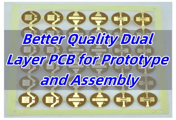
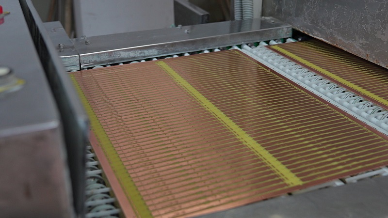
EBest Circuit (Best Technology) is a China EMS PCB manufacturer, presenting better quality dual layer PCB for prototype and assembly service to worldwide clients and markets. Our standard process for double layer PCBs supports a minimum finished board thickness of 0.2mm ±0.1mm, compatible with ENIG surface finish. For special requirements, we can produce boards with thicknesses ranging from 0.15mm to 0.4mm (±0.1mm) within a maximum size of 350×350mm. Our rigid PCB line varies, including heavy copper PCB, extra thin PCB, high Tg PCB, HDI PCB, and RF PCB. For any help, please contact our team by calling +86-755-2909-1601 or email at sales@bestpcbs.com.
What is a Dual Layer PCB?
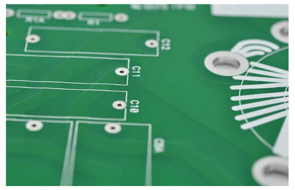
A dual layer PCB, also called a double-sided PCB, has two copper layers—one on the top and another on the bottom. These layers are connected by plated through-holes. This structure allows for denser routing and more components compared to single layer boards. Dual-layer PCBs strike a strong balance between simplicity and capability.
What is the Difference Between Single and Double Layer PCB?
Single layer PCBs have components and routing only on one side. They are simple, low-cost, and easier to produce. But they can be limiting in complex circuits. Dual layer PCBs, by contrast, offer routing on both sides, providing more space and better electrical performance. For example, you can separate power and signal traces better, which improves noise control and makes debugging easier.
What is the Difference Between Dual Layer PCB and 4 Layer PCB?
A dual layer PCB has two copper layers, while a 4-layer PCB includes additional inner layers, usually for power and ground. This extra space gives better EMI shielding and more routing options. But it comes at a higher cost and longer lead time. Unless the circuit requires that added complexity, dual-layer designs are often more practical for cost-sensitive applications.
What are 2-Layer PCB Design Rules?
Effective design helps avoid signal problems and manufacturing defects. For a 2-layer PCB, key rules include:
- Route high-speed signals near a ground plane to reduce interference.
- Use decoupling capacitors near power pins to stabilize voltage.
- Ensure impedance matching for differential pairs like USB or HDMI.
- Minimize vias and layer transitions to keep costs low.
EBest Circuit (Best Technology)’s engineers help review your design before production to catch layout issues early. Our team uses automated DRC/DFM tools to prevent costly mistakes.
How Much Does a 2 Layer PCB Cost?
Prices depend on board size, copper thickness, surface finish, and order volume. On average, small batch prototype PCBs start at $30–$80, while larger production runs can bring per-unit cost below $1. At EBest Circuit (Best Technology), we offer cost control strategies like layout optimization, material selection (such as CEM-3), and bulk ordering for better pricing.
What is a Double Layer PCB Board Used For?
Double layer PCBs are used in a wide range of electronics. Common examples include:
- Power supply modules
- Lighting systems like LED drivers
- Consumer electronics like smart devices
- Industrial control boards
Their simplicity makes them easy to test and repair, yet they are robust enough for demanding use cases. With good layout, they can also handle moderate-speed signals and analog circuits.
Where to Get Dual-Layer PCB?
Choosing a reliable partner matters. EBest Circuit (Best Technology) provides dual layer PCB solutions tailored to your needs. We support prototyping, mass production, and turnkey assembly. Every board goes through electrical testing, visual inspection, and X-Ray for via quality. We also solve common pain points faced by engineers:
- EMI issues? We suggest layout improvements and material selection to reduce noise.
- Signal quality concerns? Our impedance control ensures clean signals for fast communication.
- Soldering defects? We use AOI and X-Ray to catch issues before boards ship.
- Component misalignment? Our high-precision pick-and-place equipment maintains tight tolerances.
Our MES system ensures every component and batch is traceable—improving quality and simplifying troubleshooting.
In brief, dual layer PCBs are a great choice for prototypes and production alike. They offer a balance of performance and cost. But without proper design and process control, issues like signal loss, EMI, or soldering errors may arise.
EBest Circuit (Best Technology) solves customer needs with complete solutions: from layout optimization, precision drilling, automated assembly, to final testing. Whether you’re in automotive, medical, or consumer products, our team ensures your board meets every requirement. You can contact us at sales@bestpcbs.com, and be sure to give us Gerber files, quantity, and any special requirements so that we can quote you as fast as we can.
Tags: Better Quality Dual Layer PCB for Prototype and Assembly, Dual Layer PCB