

In high-speed electronic systems, signal integrity is crucial. One of the key factors that ensures clear, distortion-free signal transmission is impedance control. In this blog, we’ll explore what impedance control is, why it’s important in PCB design, how it’s calculated, and what factors influence it. Whether you’re a PCB designer or sourcing boards from a manufacturer, understanding impedance control is essential to ensuring performance and reliability.

What Is Impedance in a PCB?
Impedance refers to the resistance a circuit offers to alternating current (AC), especially in the presence of inductors and capacitors. In simple terms, it’s how much the signal “fights back” as it moves through the traces on a PCB. The unit of impedance is Ohms (Ω).
In PCBs, impedance isn’t just about resistance—it includes the effects of capacitance and inductance created by the PCB’s structure and materials. That’s why it needs to be tightly controlled, especially in high-speed signal circuits.
Why Is Impedance Matching Needed?
Impedance matching is essential to ensure efficient signal transmission across different parts of an electrical system. When the impedance of a signal source, transmission path (such as a PCB trace), and load are not properly matched, it causes signal reflection, power loss, and distortion—especially in high-speed or RF designs.
Key reasons why impedance matching is necessary:
- Prevents Signal Reflection: Any mismatch causes part of the signal to bounce back to the source, interfering with the original signal and creating noise.
- Maintains Signal Integrity: For data to reach its destination accurately and consistently, impedance must be uniform along the transmission path.
- Reduces EMI (Electromagnetic Interference): Mismatched impedance can result in radiated emissions, which may interfere with nearby circuits.
- Improves Power Transfer: In RF applications, maximum power is transferred only when the source and load impedance are equal.
- Enables High-Speed Communication: Interfaces like HDMI, USB, Ethernet, and LVDS require tight impedance control for proper function.
In short, impedance matching is critical to achieving predictable, reliable performance in complex circuits and high-speed digital or RF systems.
What Is Impedance Control?
Impedance control is the process of designing PCB traces so that their impedance remains within a specified tolerance, typically ±10%. This ensures signal transmission remains clean, reduces signal reflections, and avoids data loss or distortion—especially critical for USB, HDMI, high-speed memory, and RF circuits.
Why Is Impedance Control Important?
Controlled impedance becomes essential in high-frequency applications like:
- Communication equipment
- Medical devices
- Aerospace and defense electronics
- Consumer electronics
- Automotive systems
Signals traveling through improperly matched impedances can reflect back toward the source, leading to noise, jitter, and signal loss.
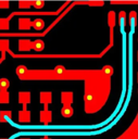
Common Types of PCB Impedance
Impedance isn’t a one-size-fits-all metric. There are different types, depending on signal configuration:
1. Single-Ended Impedance (Single-Ended Trace)
This refers to the impedance of a single signal line with respect to a reference plane (usually GND). This type is common in basic digital or analog signals.
Example: 50Ω impedance, line width of 5 mil on L1 referencing L2.

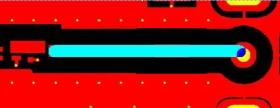
2. Differential Impedance
Used in differential pair routing where two lines carry equal and opposite signals (like in USB, HDMI). The impedance is measured between the two lines.
Example: 90Ω impedance, line width/spacing = 5/6 mil, referencing L2.
3. Coplanar Impedance
Here, the signal line is flanked by ground or power planes on the same layer, adding shielding and tighter impedance control.
- Single-Ended Coplanar Impedance: Signal line with ground on both sides.
- Differential Coplanar Impedance: Differential pair surrounded by ground on the same layer.
Example: 90Ω impedance, line width/spacing = 7.5/8/8 mil.
How Is Impedance Calculated?
Impedance is calculated using simulation tools that factor in geometry and material properties. The most commonly used tools include:
- Polar SI8000
- Polar SI9000

These tools allow engineers to model various stack-ups and design constraints to meet impedance targets.
- Common input parameters include:
- Trace width
- Trace spacing (for differential)
- Distance to reference plane (dielectric thickness)
- Dielectric constant (Dk)
- Copper thickness
Factors That Affect Impedance in PCB Design
Controlling impedance means adjusting several design parameters. Here’s how they influence impedance:
| Factor | Effect on Impedance |
| Line width | Wider lines reduce impedance (inverse) |
| Line spacing | Narrower spacing lowers differential impedance |
| Dielectric thickness | Thicker dielectric increases impedance |
| Distance to nearby copper | Greater distance increases impedance |
| Dielectric constant (Dk) | Higher Dk reduces impedance |
| Copper thickness | Typically fixed; indirectly affects trace width needs |
In practice, designers will tweak line width, spacing, and dielectric thickness to reach target values, since Dk and copper thickness are often constrained by material availability or cost.
Impedance Control Verification
Impedance control verification is the process of measuring and confirming that the actual impedance on the manufactured PCB matches the design specifications. This verification ensures that the board will perform reliably in the intended high-speed application. Here are some verify impedance control methods:
1. Test Coupons:
- Special trace structures are added to the edge of the production panel.
- These are manufactured using the same stack-up and process as the main board.
2. TDR (Time Domain Reflectometry):
- A signal pulse is sent through the test coupon trace.
- The equipment measures how the signal reflects along the trace to determine actual impedance.
- This method is non-destructive and very precise.
3. Report & Tolerance Check:
- The measured values are compared against target impedance (e.g., 50Ω, 90Ω).
- Typical tolerance is ±10%, depending on customer requirements.
- A formal impedance test report is provided.
4. Process Adjustments (if needed):
If values fall outside tolerance, manufacturers may tweak line width or dielectric thickness and re-run tests before final production.
Verifying impedance isn’t just a formality—it’s a guarantee that the board will function correctly in its application. Skipping this step can result in field failures, EMI issues, or complete communication breakdowns.
Why Choose EBest Circuit (Best Technology) for Impedance-Controlled PCBs?
At EBest Circuit (Best Technology), we specialize in high-speed, high-reliability PCBs with precise impedance control. We use industry-standard impedance calculation software and fabricate test coupons to verify every impedance-controlled design. Whether you need simple 2-layer PCBs or complex HDI PCB stackups with tight tolerances, we provide:
- Competitive pricing
- Rigorous quality control
- Engineering support for stackup & impedance design
- Fast lead times
FAQs About Impedance Control
1. What is the typical tolerance for controlled impedance?
Most designs require ±10% tolerance from the target impedance value.
2. Do all PCBs require impedance control?
No, only high-speed or RF boards need impedance-controlled traces.
3. How do manufacturers verify impedance control?
They use test coupons and tools like TDR (Time Domain Reflectometry).
4. Can I use FR4 for impedance-controlled designs?
Yes, but its dielectric constant must be accounted for in calculations.
5. What happens if impedance isn’t controlled?
It can lead to signal reflection, data loss, and poor system performance.