
China heavy copper PCB is not just about thicker copper layers. It’s a complete solution to manage high current, heat, and mechanical stress in demanding electronic systems. For engineers and buyers who need reliability, fast prototyping, and reduced risk, heavy copper PCBs from trusted Chinese manufacturers are becoming essential. This article dives into what makes them special and how to choose the right partner for your next project.
Best Technology is one of the leading heavy copper PCB manufacturers in China, providing pre-sales support, prompt prototyping, and assembly service. We trust that rapid prototyping, extraordinary quality, turnkey EMS PCB solutions, and efficient delivery are prerequisites for us to establish long-term competitiveness and win customer loyalty in international markets. Per our no-procrastination culture, we adhere to the principle of ensuring efficiency from the top down: Today’s work must be done today. That accelerates the time of your final product entry. As a customer-driven factory, your satisfaction is the priority at BEST. If you are interested in our heavy copper PCBs, please contact us via our contact link here.
What Is the China Heavy Copper PCB?
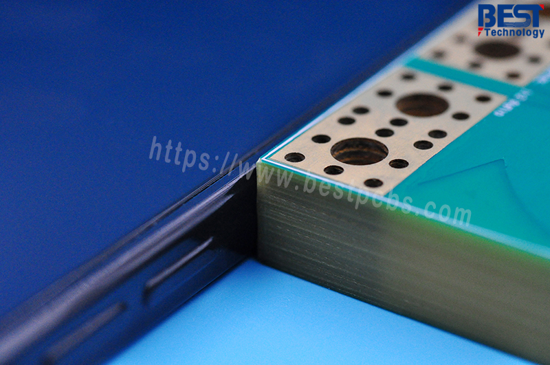
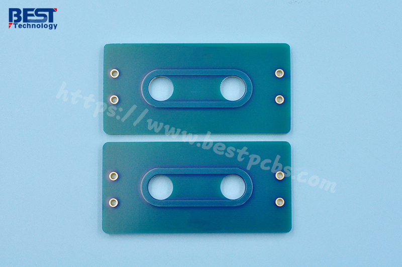
Heavy copper PCBs are built with copper layers thicker than the standard 1oz. These boards often carry 2oz to 6oz copper thickness, but they can go beyond that depending on the application. When made in China, these boards benefit from scalable production and cost-effective services. The increased copper allows better current flow, improved thermal performance, and stronger physical integrity.
What Is the Manufacturing Process for China Heavy Copper PCB 4Layer?
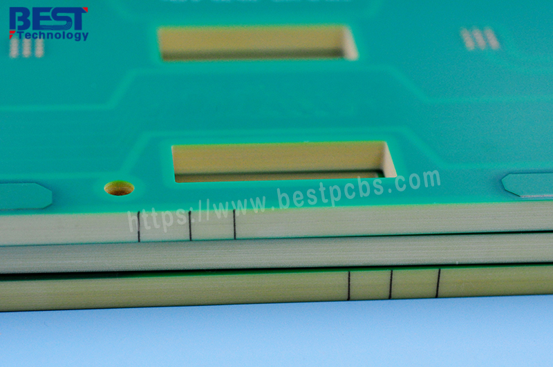
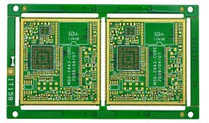
Producing a China heavy copper PCB 4layer requires precision. Each layer starts with high-quality base material. Then copper is laminated and etched carefully. Plating is strengthened with optimized electroplating formulas. The multi-layer bonding process uses step-by-step lamination to prevent resin voids. Special drilling equipment and tight process control avoid misalignment and burrs. Every step is monitored to avoid surface roughness and inner layer shifting.
What Are the Advantages of China Heavy Copper PCB?
The benefits go beyond durability. Here are the key advantages:
- Current Handling: Increased copper means better current-carrying capacity.
- Thermal Control: Heat spreads faster, protecting key components.
- Mechanical Strength: Boards resist vibration and mechanical stress.
- Multilayer Support: Complex layouts become manageable.
- Long Life: Boards last longer, even in tough environments.
What Are the Applications for Heavy Copper PCB?
Heavy copper PCBs are used in industries that need strength and stability:
- Power Electronics: Used in solar inverters, UPS, and charging stations.
- Industrial Control: Drives, sensors, robotics, and automation equipment.
- Aerospace: Suitable for high-reliability aircraft systems.
- Automotive: Key for EV battery management and control systems.
- Medical: Critical for stable readings in pH meters, ECG devices, and more.
China Heavy Copper PCB Manufacturers
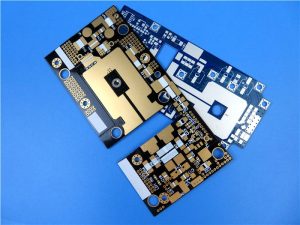
Many Chinese PCB manufacturers now specialize in heavy copper PCB production. However, not all meet the tight tolerance, flatness, and plating standards required. Common complaints include board warping, resin issues, and poor copper fill in holes. Reliable heavy copper PCB manufacturers in China use real-time monitoring systems, better resin control, and balanced copper distribution across layers. Below are three trusted manufacturers in China known for their strong track records in this field.
1. Best Technology
Best Technology stands out for its expertise in producing multilayer heavy copper PCBs with up to 10oz copper thickness. What sets them apart is their step-lamination technique, which helps manage uneven copper areas and reduces surface warping during SMT. With in-house DFM support and smart MES tracking systems, Best also delivers fast prototyping—an edge that matters in time-sensitive projects. We are certified to ISO 9001, IATF 16949, AS9100D, and ISO 13485, covering industries from automotive to aerospace and medical.
2. Suntak Technology
Suntak is one of China’s large-scale PCB manufacturers, offering advanced capabilities in high-power circuit board production. They have robust equipment for thick copper etching and are known for their strict quality checks at each production stage. Their automated production lines reduce manual errors, helping ensure flatness and consistent copper plating, especially in 4–6 layer designs used in power electronics.
3. Wus Printed Circuit Co., Ltd.
Wus is a long-established Chinese PCB maker that supplies to industrial and automotive customers worldwide. They have deep technical experience in thermal management PCBs and offer solid process control for heavy copper builds. Their ability to handle complex multilayer stackups and copper plating thickness consistency makes them a reliable option for high-reliability applications.
In summary, the demand for China heavy copper PCB production is growing, but so are the challenges—especially in heat distribution, plating reliability, and delivery time. Working with proven manufacturers like Best Technology, Suntak, and Wus gives engineering teams the confidence that their boards will meet both electrical and mechanical expectations. Among these, Best Technology offers an edge in rapid prototyping, advanced lamination processes, and responsive customer support—making it a dependable choice for businesses needing speed and precision.
How Do Heavy Copper PCB Manufacturers Ensure Prompt Prototyping?
Prompt delivery matters. Advanced Chinese factories tackle this challenge by:
- DFM Collaboration: Designs are reviewed early to avoid delays.
- In-house processes: From lamination to final testing, everything is under one roof.
- Material reserves: Strategic copper and resin storage avoid shortages.
These steps help cut turnaround time while improving consistency.
Why Choose Best Technology for China Heavy Copper PCB?
Many clients choose Best Technology for heavy copper PCB solutions—and with good reason. Here’s why:
- Manufacturing Confidence: Advanced plating control avoids poor copper in hole walls and ensures stable conductivity.
- Surface Flatness: Even when copper thickness varies, their step-by-step lamination process keeps the board flat for SMT.
- Warpage Prevention: Optimized resin ratios and lamination methods reduce PCB deformation during soldering.
- Speed: In-house DFM experts and intelligent MES systems help shorten sampling cycles.
- Quality Commitment: All boards pass AOI, X-ray, and final electrical tests.
- Certifications: ISO9001, IATF16949, ISO13485, and AS9100D show our industry expertise.
In addition, Best Technology keeps a flexible supply chain and price control through long-term supplier partnerships. With the growing copper price and customer urgency, that’s a big plus.
In a nutshell, as the need for high-power, high-reliability electronics grows, China heavy copper PCB manufacturing is rising to meet demand. But high copper content brings challenges like thermal imbalance, copper height gaps, and plating risks. Best Technology offers targeted solutions through proven processes, professional DFM support, and steady supply chains. We are the original manufacturer of China Heavy Copper PCB for Prompt Prototyping. We have our production line. Our team helps turn design into product—fast and reliably. That’s the edge buyers are looking for today. If any pertinent Heavy Copper PCB demands or would like to visit our factory, a warm welcome to contact us via email at sales@bestpcbs.com, or by giving us a call at +86-755-2909-1601.
You may also like

Tags: China Heavy Copper PCB, China Heavy Copper PCB for Prompt Prototyping