
May some engineers or designers who be interested in thick film ceramic circuit are curious about can thick film ceramic boards design with via holes like FR4 PCB? Herein, we will explore the feasibility of using thick film ceramic boards for via holes, including the materials and processes involved, as well as the advantages of this approach.
What is thick film ceramic board?
The “Thick Film” refers to the thickness of conductor layer on a Ceramic PCB. Normally the thickness will be at least 10um, around 10~13um, which is thicker than spurting technology in Thin Film Ceramic PCB. And of course thickness is less than DCB Ceramic board or FR4 board.
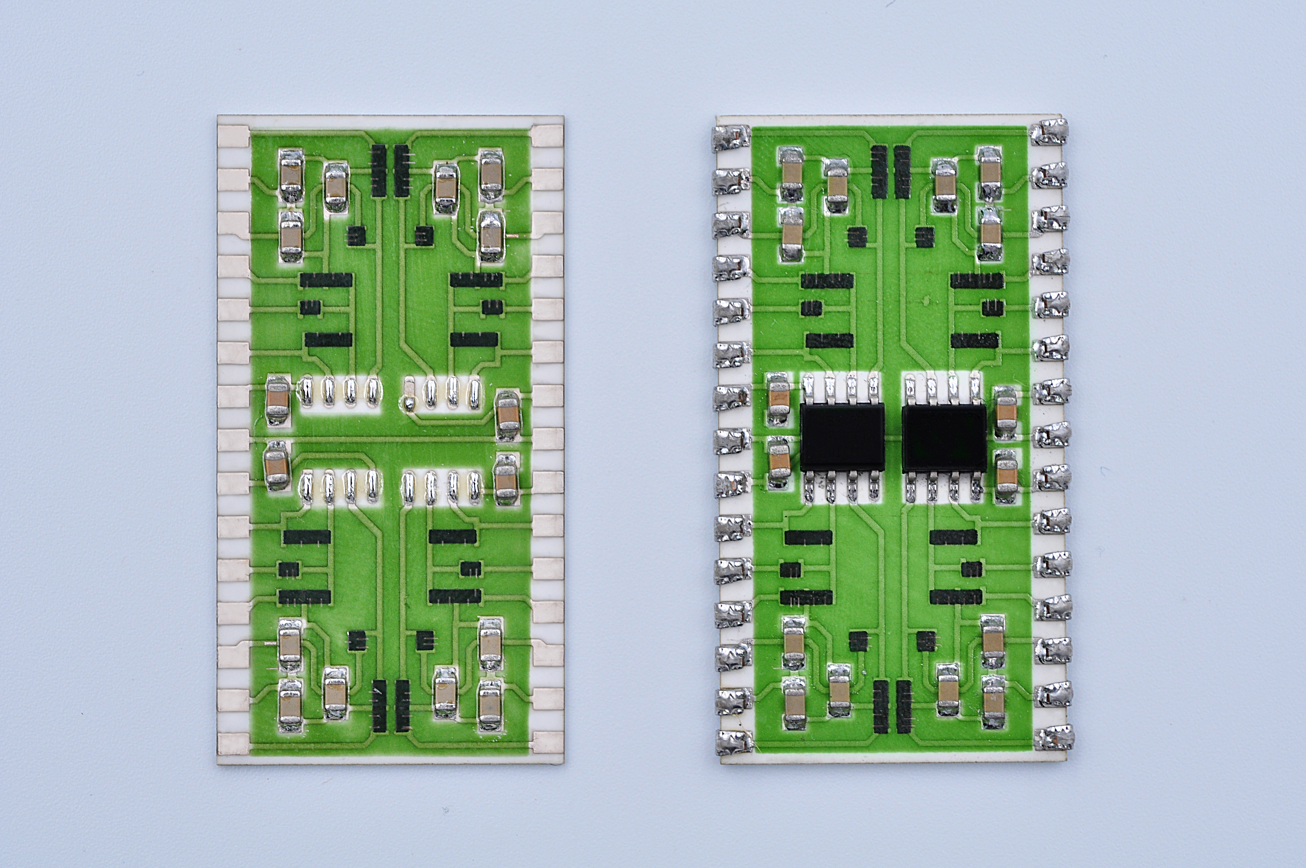
Thick film ceramic circuit enables to put resistor, electric capacitor, conductor, semi-conductor, and interchangeable conductor on ceramic board, after manufacturing steps of printing and high temperature sintering. The more important thing is by using thick film technology, we can make all the resistors with the same value, or different value for different resistor on the same board.
Materials and processes for via holes
In general, thick film ceramic circuit is not suitable for designing via holes. Because the characteristics of thick film ceramic board mainly depends on the insulation properties of its ceramic substrate, rather than conductive properties. The conductivity of thick film ceramic plate is not good than Metal Core PCB, or even we can say it has a very poor conductivity, usually can’t meet the requirements of the via hole.
But, designing via holes in thick film ceramics is available in Best Technology. Generally speaking, the fabrication of via holes in thick film ceramic boards typically involves several key materials and processes.
From the designer’s perspective, a conductive material is used to create a continuous conductive path from one side of the ceramic board to the other. Common conductive materials include gold paste, silver paste, and copper paste. These materials are usually screen printed onto the ceramic board in the desired pattern, and then fired at high temperatures to achieve sintering and form a conductive layer.
Once the conductive layer is formed, the via holes are created by drilling or punching small holes through the ceramic board at the desired locations. These holes are then filled with a conductive material, such as silver paste or copper paste, to establish electrical connections between the different layers of the circuit.
Finally, the via holes are fired again at high temperatures to achieve sintering and ensure good adhesion and electrical performance.
Advantages of Via Holes in Thick Film Ceramic Boards
These via holes offer several advantages in the design and fabrication of thick film ceramic boards, including as following:
- Electrical connectivity
Via holes provide electrical connectivity between different layers of a thick film ceramic board. They allow for the interconnection of different circuitry or conductive layers, enabling the flow of electrical signals or power between different parts of the board. This allows for complex and multi-layered circuit designs, which can be highly beneficial in applications that require intricate circuitry or high-density interconnects.
- Space-saving
Via holes can provide a means of vertical interconnection, allowing for more efficient use of board real estate. Instead of routing traces or conductors on the surface of the board, which can take up valuable space, via holes can be used to route connections through the board, freeing up surface area for other components or functions. This is especially advantageous in compact or miniaturized electronic devices where space is limited.
- Thermal management
Via holes can aid in thermal management in thick film ceramics. They can be used to transfer heat from one layer of the board to another, helping to dissipate heat generated by components or circuits. This can be particularly important in high-power or high-heat applications, where efficient thermal management is crucial for preventing overheating and ensuring reliable performance.
- Mechanical stability
Via holes provide additional support and reinforcement to the board, reducing the risk of warping, bending, or cracking. Via holes can also help improve the overall mechanical integrity of the board by reducing stress concentration points and enhancing its structural rigidity.
- Design flexibility
Via holes offer design flexibility in thick film ceramic boards. They can be designed and placed according to the specific requirements of the circuit or system, allowing for customized and optimized designs. Via holes can be used to route traces, create vias for component mounting, or provide grounding or shielding, among other functionalities. This flexibility in design allows for more efficient and effective circuit layouts, which can lead to improved performance and reliability.
As previously mentioned, designing via holes in thick film ceramic boards offers various benefits. However, when it comes to choosing the appropriate paste for via holes, silver paste is often recommended to our customers. But why is that? Can I use gold or copper? In our upcoming article, we will delve into the reasons behind this recommendation and provide you with valuable insights. Stay tuned to uncover the answers!
You may also like


Tags: ceramic PCB