
According to our earlier blogs about SinkPAD introduction,
we can know that the high power LED’s thermal pad can touch the convexity area of copper core directly, so the heat of LED will be dissipated into the air much faster and more efficient than conventional MCPCB, but if only the LED pad can be designed as SinkPAD?
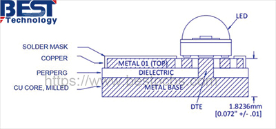
Actually the pads of other chips or components also can be designed as SinkPAD, one of the most common is the IC pad. In some designs, IC needs to pass through the large current, so it will emit a lot of heat.
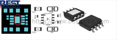
In order to dissipate heat in time, some customers will directly design the IC solder pad as sinkpad to directly contact the copper base, so that the life cycle will be longer.
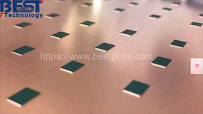
As you can see the following picture, it’s the copper layer after doing Etching, the area with blue film we normally named it as convexity, the thermal pad of IC will touch the convexity directly to achieve the purpose of dissipating the heat very fast.
If you have other questions about SinkPAD, welcome to contact Tammy (Email:sales9@bestpcbs.com), she will prove you professional suggestions and solutions.
In the end, I’d like to share the manufacturing process of SinkPAD Board with you, please Click here: SinkPAD-Board-Manufacturing-Process-Best-Technology.pdf
You may also like


Tags: SinkPAD