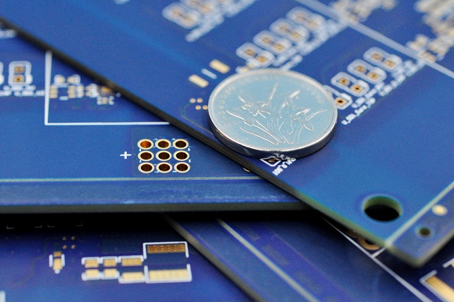
Printed Circuit Boards (PCBs) come in a variety of layer configurations and thicknesses, each suited to specific electrical and mechanical needs. One of the most common total thicknesses in the industry is 1.6mm, but depending on copper weight and dielectric material selection, the actual thickness can vary—sometimes leaning closer to 1.7mm, especially in high copper-weight designs.
A Closer Look at 6-Layer PCBs with Heavy Copper
For example, a 6-layer PCB with 4oz copper on all layers and a nominal thickness of 1.6mm can practically reach 1.68mm. This is because each 4oz copper layer measures about 35µm, and the dielectric materials—commonly Prepreg (PP)—must be of equal or compatible thickness to match the structural and electrical integrity.
Thickness Calculation Example:
- 4oz copper ≈ 140µm per layer (both sides)
- Dielectric material (PP) thickness ≈ matches the copper layers
- Total stack-up: 4oz × 35µm × 6 layers × 2 (copper + PP) = ~1.68mm
Such a construction is ideal when higher current-carrying capacity, thermal performance, and mechanical strength are required—for example, power distribution boards, automotive controllers, and industrial automation equipment.
When More Layers Matter: 12-Layer PCBs and Beyond
As systems grow more complex, 12-layer PCBs are commonly used in high-speed data communication, AI computing platforms, and server mainboards. These applications require not only signal integrity but also EMI shielding, controlled impedance, and dedicated power/ground planes.
- A 12-layer stack-up typically includes:
- Multiple signal layers for differential pairs and high-speed routing
- Dedicated ground and power planes
- Carefully chosen PP and core materials to maintain target thickness (often still around 1.6mm)
Maintaining 1.6mm with more layers means thinner individual dielectric layers and copper foils, making material selection and lamination control critical.
Thickness, Materials, and Dielectric Strength
The interplay between copper thickness, prepreg, and core materials affects not only the final PCB thickness but also electrical isolation and breakdown voltage. Thicker copper increases current capacity but reduces the available space for dielectric layers—potentially compromising dielectric strength if not properly managed.
To ensure breakdown voltage requirements are met, manufacturers must:
- Use high-quality, high-resin content prepregs
- Maintain minimum dielectric spacing between high-voltage nets
- Control resin flow during lamination to avoid thin spots
For example, FR-4-based PCBs typically require at least 100µm spacing to withstand 500V or more, depending on the resin system.
Conclusion
While 1.6mm is a standard thickness in PCB manufacturing, the internal layer structure determines the real-world electrical and mechanical performance. From 6-layer power boards with 4oz copper to 12-layer high-speed boards, designers must strike a balance between copper weight, material thickness, and breakdown strength.