Seeking for PCB fabrication specifications? This guide covers all critical aspects from material selection to final panel dimensions for reliable PCB manufacturing.
With 18+ years of PCB manufacturing expertise, Best Technology delivers reliable solutions through standardized production processes, every operation follow PCB fabrication specifications to ensure consistency. Our advanced manufacturing capabilities support all surface finishes (ENIG, OSP, immersion silver/tin) and specialty boards including HDI (up to 20 layers), RF (controlling εr ±0.2), and heavy copper board (6oz+). Competitive pricing with transparent cost structures eliminates hidden fees, while 100% batch inspection guarantees defect rates below 500ppm. We can achieve 24-hour prototype turnaround (from Gerber to shipment) and volume production lead times 30% shorter than industry averages, enabling clients to accelerate time-to-market. For high-mix applications from 5G antennas to industrial controllers, our engineering team resolves fabrication challenges through adaptive process optimization. Welcome to contact us for a quote now: sales@bestpcbs.com.
Definition of PCB Fabrication Specifications
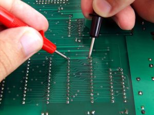
PCB fabrication specifications define the precise technical requirements for manufacturing printed circuit boards, encompassing material properties, dimensional tolerances, processing methods, and quality validation criteria. These specifications document essential parameters such as laminate material grades, copper weight tolerances (typically ±10%), drilling positional accuracy (±0.05mm standard), plating thicknesses (25μm minimum for through-holes), solder mask application standards (15-25μm LPI thickness), and surface finish requirements (e.g., ENIG with 3-5μm nickel layer). They establish testing protocols including impedance control verification (±10% tolerance), microsection analysis for plating quality, and IPC Class 2/3 acceptance criteria for visual defects. The specifications also address panelization rules (V-cut depth tolerances), environmental conditioning procedures (thermal stress testing), and final packaging standards (moisture barrier bags with desiccant). By systematically defining these manufacturing parameters, PCB fabrication specifications ensure consistent production quality while maintaining compatibility with assembly processes and end-use operating conditions.
Substrate for PCB Fabrication Specifications
Below are substrate for PCB fabrication specifications :
- Dielectric Constant (Dk) Stability: Choose materials with consistent Dk values across frequencies to minimize signal distortion. For high-speed designs, low-Dk laminates (e.g., 3.2–3.8) reduce propagation delays, ensuring timing accuracy in applications like 5G or servers.
- Thermal Management Capabilities: Prioritize high thermal conductivity (e.g., 0.8–2.0 W/m·K) for power electronics or LED boards to prevent overheating. Materials with decomposition temperatures (Td) above 300°C withstand lead-free soldering without delamination or warping.
- Moisture and Chemical Resistance: For automotive or outdoor devices, select substrates with low moisture absorption (<0.1% per IPC-TM-650) to avoid swelling, delamination, or electrical leakage. Chemical-resistant finishes further enhance durability in harsh environments. Mechanical Strength and Flexibility: Rigid-flex designs require polyimide or similar flexible substrates with high tensile strength (e.g., >200 MPa) to endure bending cycles without cracking. Rigid boards may use FR-4 or high-Tg epoxy for structural stability.
- Impedance Control Requirements: Materials with tight dielectric thickness tolerances (e.g., ±5%) ensure consistent impedance for differential pairs or RF traces. This precision prevents reflections and signal integrity issues in high-frequency circuits.
- Cost vs Performance Balance: Thicker foils increase material costs by ~15–30% per step but reduce resistive losses in power electronics.
Copper Foil Thickness & Tolerance For PCB Fabrication Specifications
Copper foil thickness and tolerance of PCB fabrication specification:
- Standard Thickness Options: Covers common weight classes: ½ oz (17.5 µm), 1 oz (35 µm), 2 oz (70 µm), and 3 oz (105 µm) per square foot. Thinner foils (≤½ oz) suit high-density designs, while thicker foils (≥2 oz) handle high-current traces.
- Manufacturing Tolerances: Specifies ±10% thickness tolerance for rolled/electrodeposited foils post-etching. Tighter tolerances (±5%) are achievable for impedance-controlled layers through process controls.
- Surface Roughness Parameters: Defines peak-to-valley roughness (Rz ≤5 µm for standard foils, ≤1.2 µm for low-profile RF applications) to balance adhesion and high-frequency signal integrity.
- Ductility and Elongation: Requires elongation rates >8% for flexible circuits to withstand bending, while rigid PCBs typically tolerate 3–5% elongation.
- Current-Carrying Capacity: Correlates thickness with ampacity: 1 oz foil supports ~1A per 10 mil trace width at 10°C temperature rise, scalable for thicker foils.
- Impedance Control Implications: Thickness variations directly affect trace impedance. A ±7% thickness shift may cause ±2Ω deviation in 50Ω designs, necessitating tighter controls for high-speed layouts.
- Plating Compatibility: Ensures foil surfaces accommodate subsequent copper plating (e.g., 25 µm hole wall plating) without delamination risks through adhesion testing.
Drilling & Routing Tolerances Specification For PCB Manufacturing
Drilling and routing tolerances of PCB fabrication specification:
- Drilling & Routing Tolerances Specifications: Here’s a structured breakdown of Drilling & Routing Tolerances Specifications for PCB fabrication, designed for clarity and practical application:
- Hole Diameter Tolerance: Standard drilled holes maintain ±0.05 mm (±2 mil) tolerance for diameters ≥0.3 mm, while microvias (<0.15 mm) require tighter controls (±0.025 mm). Laser-drilled holes achieve ±0.01 mm precision for HDI designs.
- Hole Position Accuracy: Specifies ±0.075 mm (±3 mil) positional tolerance relative to datum, critical for multilayer registration. Optical alignment systems reduce this to ±0.05 mm for high-density interconnects.
- Routing Edge Tolerance: Outlines ±0.1 mm (±4 mil) tolerance for board outlines and cutouts, with ±0.05 mm achievable for RF shields or press-fit components.
- Aspect Ratio Limits: Defines maximum 10:1 aspect ratio for mechanical drilling (e.g., 0.3 mm hole depth for 0.03 mm diameter), extending to 15:1 with laser drilling.
- Burr and Roughness Standards: Requires hole wall roughness <25 µm Ra to ensure uniform plating adhesion, with burr height <50 µm to prevent solder masking issues.
- Slot Width and Spacing: Controls slot widths (±0.1 mm tolerance) and minimum 0.2 mm spacing between adjacent routed features to avoid mechanical stress fractures.
- Tool Wear Compensation: Accounts for drill bit wear (±0.02 mm diameter increase per 1,000 hits) through automated diameter correction systems.
- Material-Specific Considerations: Adjusts feed rates for FR-4 (0.8–1.2 m/min) versus ceramic substrates (0.3–0.5 m/min) to minimize smearing or cracking.
Plating Thickness Standards
Here’s a practical breakdown of plating thickness standards:
- Copper Plating for Through-Holes & Vias: Specifies 25 µm (1 mil) minimum thickness for hole walls to guarantee electrical connectivity and mechanical durability. Thinner deposits (<20 µm) risk cracking during thermal cycling, while excessive plating (>35 µm) may cause uneven current distribution.
- Surface Finish Thickness (ENIG, HASL, etc.): Gold over nickel (ENIG): 0.05–0.10 µm gold atop 3–5 µm nickel to prevent oxidation without compromising solderability. HASL (tin-lead/lead-free): 1–25 µm coating to ensure even solder wetting while avoiding bridging.
- Edge Connector Plating: Demands 50–75 µm hard gold over 2–3 µm nickel for high-wear areas, ensuring 10,000+ mating cycles without degradation.
- Flexible Circuit Requirements: Limits copper plating to 12–18 µm for dynamic flex regions to prevent fatigue fractures, paired with 2–3 µm nickel underplate for stress relief.
- High-Current Traces & Planes: Recommends 35–70 µm copper for power layers to minimize resistive losses, verified by cross-sectional microscopy.
- Plating Uniformity Tolerance: Enforces ±10% thickness variation across panels, measured via X-ray fluorescence (XRF) to avoid impedance mismatches in high-speed designs.
- Plating Adhesion Testing: Requires >1.5 N/mm peel strength per IPC-6012 to withstand assembly processes like reflow soldering.
- Cost vs Performance Balance: Thicker platings increase material costs by ~20% per 10 µm but reduce field failures in harsh environments (e.g., automotive underhood).
Solder Mask Specifications
Here are the solder mask for PCB fabrication specifications presented in clear:
Material Properties
- Standard liquid photoimageable (LPI) epoxy-based solder mask
- UL 94V-0 flammability rating for safety compliance
- Dielectric strength >1000V/mil for electrical insulation
- Thermal resistance up to 150°C for lead-free soldering processes
Thickness Specifications
- 0.5-1.0 mil (12.5-25μm) over conductors
- 0.8-1.5 mil (20-38μm) over laminate surfaces
- Minimum 0.3 mil (8μm) in any area
Color Options
- Standard colors: green, red, blue, black, white
- Custom colors available with 10% additional cost
- Matte and glossy finishes selectable
Registration Tolerance
- ±3 mil (76μm) for standard designs
- ±2 mil (51μm) for high-precision boards
- Alignment marks required for tight-tolerance designs
Opening Requirements
- Minimum solder mask opening: 4 mil (100μm)
- Web width between openings: 3 mil (75μm) minimum
- Tented vias permitted with 5 mil (125μm) annular ring
Surface Finish Compatibility
- Compatible with HASL, ENIG, OSP, Immersion Silver
- Special formulations available for flexible PCBs
- No interaction with final surface finishes
Curing Process
- UV exposure followed by thermal cure
- Full cure at 150°C for 60 minutes
- Post-cure hardness: >6H pencil hardness
Quality Standards
- IPC-SM-840 Class 3 compliant
- No pinholes, bubbles, or uncured areas
- Adhesion passes tape test per IPC-TM-650
Special Features
- Peelable mask option available
- Selective thickness variation possible
- Edge clearance: 10 mil (250μm) from board outline
Surface Finishes Requirements
Surface Finish Requirements for PCB Fabrication:
HASL (Hot Air Solder Leveling, Lead-Free)
- Thickness: 1–40 µm (minimum 1 µm over copper).
- Profile Control: Dome height ≤15 µm for components with pitch ≤0.65 mm.
- Cleanliness: Zero visible flux residue post-processing.
ENIG (Electroless Nickel Immersion Gold)
- Nickel Thickness: 3–5 µm with phosphorus content 8–12%.
- Gold Thickness: 0.05–0.10 µm (99.9% purity minimum).
- Reliability: Pass IPC-J-STD-003 solderability testing after 155°C thermal aging.
Immersion Tin (ImmSn)
- Thickness: 0.8–1.2 µm uniformly coated.
- Shelf Life: 6 months in nitrogen-sealed packaging.
- Handling Protocols: Glove-only contact to prevent oxidation.
Immersion Silver (ImmAg)
- Thickness: 0.2–0.5 µm with ≤0.1 µm variation.
- Tarnish Prevention: Sulfur-free vacuum packaging required.
- Microvoid Control: ≤5% voiding in post-reflow cross-sections.
Electrolytic Hard Gold
- Nickel Underlayer: 1.5–2.5 µm minimum.
- Gold Thickness: 0.5–1.27 µm (cobalt-hardened).
- Durability: Withstand 200+ insertion cycles without wear.
OSP (Organic Solderability Preservative)
- Coating Thickness: 0.2–0.5 µm verified by colorimetry.
- Assembly Window: Single reflow cycle recommended.
- Storage: Dry cabinet (<30% RH) with 6-month expiration.
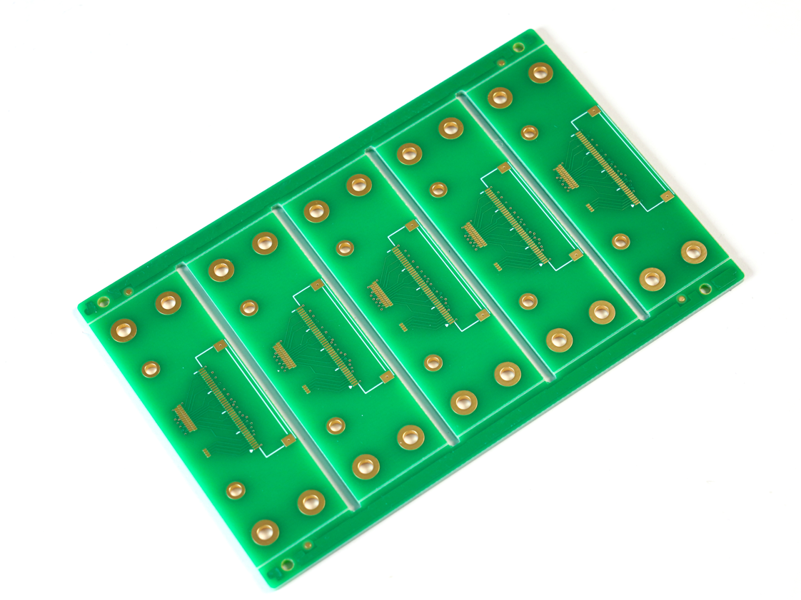
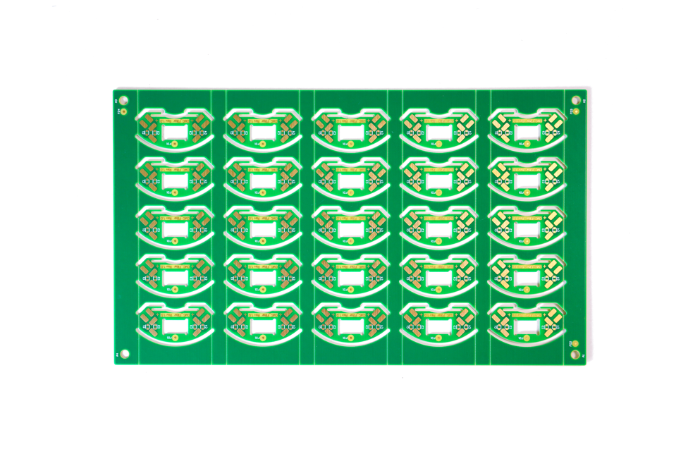
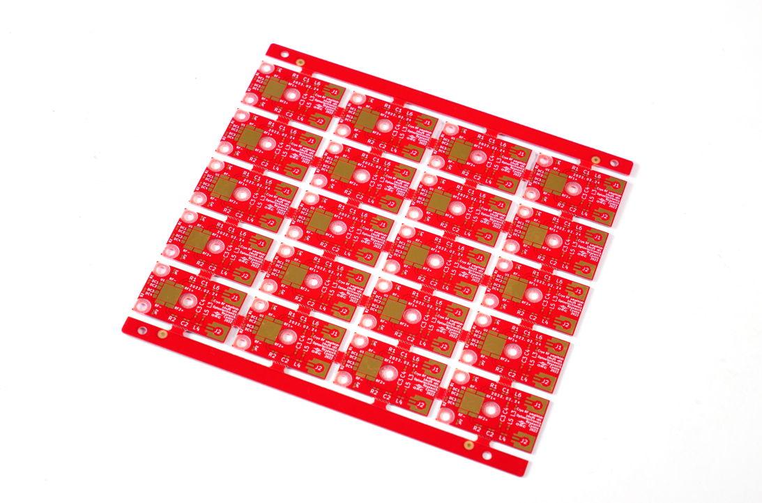
PCB Fabrication Panelization Size Specifications
PCB Fabrication Panel Size Specifications
Standard Panel Dimensions
- Common sizes: 18″x24″, 21″x24″, 18″x21″
- Thickness range: 0.2mm to 3.2mm
- Implementation: Larger panels (24″x30″) available for high-volume production
Design Considerations
- Minimum clearance: 0.5mm between board edges and panel borders
- Tooling holes: Three 3.0mm holes minimum, placed asymmetrically
- Fiducial markers: Two global and two local markers per board
Panelization Methods
- V-cut: 0.4mm depth minimum, 30° or 45° angle standard
- Tab routing: 0.8mm minimum tab width, 2-3 bridges per side
- Perforations: 0.3mm drill holes spaced 1.0mm apart
Breakaway Tab Specifications
- Tab width: 2.0-3.0mm
- Tab spacing: 50-100mm intervals
- Tab location: Avoid placing near fine-pitch components
Material Utilization Guidelines
- Optimal board spacing: 3-5mm between individual PCBs
- Panel utilization target: 75-85% of total area
- Nesting strategy: Consider rotation (90°/180°) for better efficiency
Specialty Panel Requirements
- Flexible circuits: 12″x18″ maximum for consistent handling
- Heavy copper boards: Reduce panel size by 20% for weight management
- RF materials: Limit panel size to minimize material waste
Shipping Considerations
- Maximum shipped panel size: 24″x30″x2″
- Weight limit: 15kg per panel for safe handling
- Packaging: Edge protectors required for panels >18″ in length
Implementation Strategy
- For prototype runs: Use 18″x24″ panels with 5mm spacing
- For mass production: Optimize panel size based on monthly volume
- For mixed-technology boards: Separate rigid and flex sections into different panels
Conclusion
In conclusion, this guide has systematically covered all critical PCB fabrication specifications including material properties, copper thickness tolerances (±10% standard), drilling accuracy (±0.05mm), plating standards (minimum 25μm), and panel size optimization (18″×24″ typical). Proper implementation of these specifications ensures reliable circuit performance, manufacturing yield, and cost efficiency. For projects requiring precision execution of these technical parameters, from high-frequency boards needing tight impedance control to multilayer designs demanding exacting layer alignment. Consult Best Technology’s engineering team for competitive quotations and manufacturing solutions. Their expertise in IPC-class fabrication guarantees your designs meet both performance requirements and industry compliance standards while optimizing production costs. Request a customized quote today: sales@bestpcbs.com.