

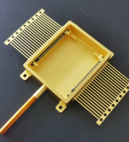
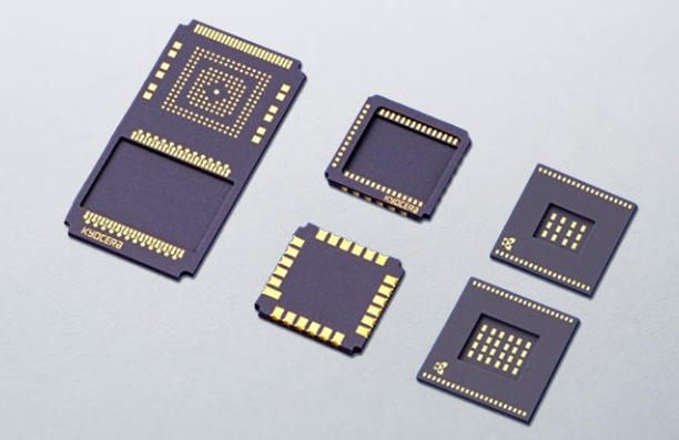
Metallized ceramic substrate is the critical foundation for high-temperature, high-power, and mission-critical electronic designs—indispensable for medical devices, aerospace systems, and industrial equipment. Selecting the right metallized ceramic substrate directly impacts thermal performance, signal integrity, and long-term reliability. This expert guide covers everything you need to know about metallized ceramic substrate, from core principles to real-world solutions and trusted manufacturing.
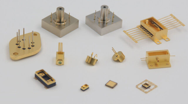
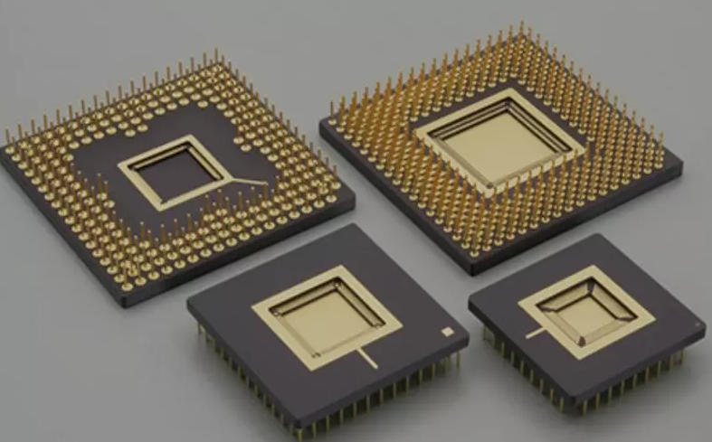
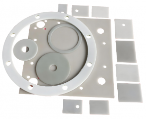
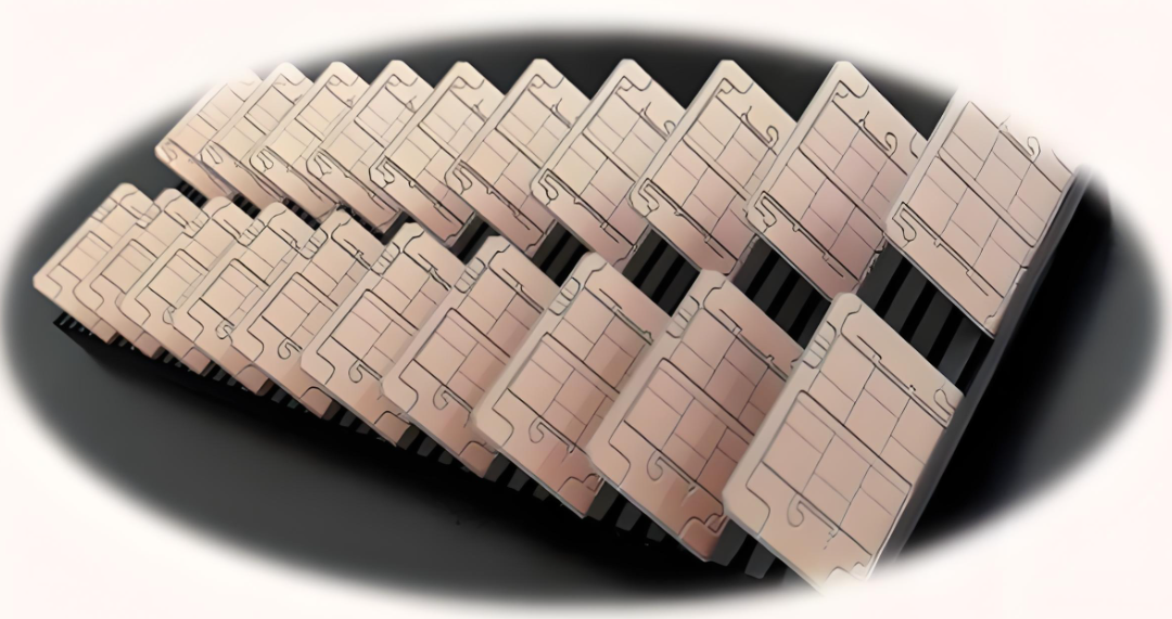
Metallized Ceramic Substrate
What Is Metallized Ceramic Substrate & How Does It Work?
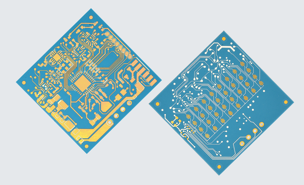
A metallized ceramic substrate consists of a ceramic base (Al₂O₃, AlN, Si₃N₄) with precision-bonded metal layers, combining ceramic’s excellent thermal conductivity and electrical insulation with metal’s electrical conductivity. It efficiently dissipates heat from high-power components, solving the thermal bottleneck of standard PCBs.
Core Structure
Ceramic insulating layer: Provides thermal dissipation and electrical isolation
Metal conductive layer: Forms circuit traces and component mounting pads
Strong metal-ceramic bond: Prevents delamination under thermal and mechanical stress
Why Use Metallized Ceramic Substrate for High-Power Electronics?
Metallized ceramic substrate delivers unmatched advantages over FR-4 and thick-film substrates in extreme operating conditions. It is the only choice for designs requiring stable performance under high heat and stress.
Key Advantages
Ultra-high thermal conductivity (up to 200 W/m·K for AlN, compared to 0.35 W/m·K for FR-4)
Excellent electrical insulation and high voltage breakdown resistance
Stable operation from -55°C to 200°C+
Low thermal expansion that matches silicon chips, reducing thermal fatigue
High mechanical strength and resistance to vibration and shock
Metallized Ceramic Substrate vs Thick Film vs Thin Film: Which Is Better?
Parameter | Metallized Ceramic Substrate | Thick Film Substrate | Thin Film Substrate
Thermal Conductivity | High (170–200 W/m·K for AlN) | Medium (10–30 W/m·K) | Low (5–15 W/m·K)
Line Precision | High (50–100μm) | Medium (100–200μm) | Ultra-High (10–50μm)
Power Handling | High (kW-level) | Medium (100W-level) | Low (10W-level)
Bond Strength | Excellent | Good | Fair
Best Application | High-power, aerospace, medical | Consumer electronics, sensors | RF, microwave, precision circuits
What Materials Are Used for Metallized Ceramic Substrate?
Three primary ceramic materials are used for metallized ceramic substrates, each with unique thermal and mechanical properties tailored to specific applications.
Alumina (Al₂O₃)
Cost-effective, high in mechanical strength, and widely adopted
Thermal conductivity: 25–35 W/m·K
Ideal for general industrial, automotive, and mid-power designs
Aluminum Nitride (AlN)
Ultra-high thermal conductivity and a near-perfect thermal expansion match with silicon
Thermal conductivity: 170–200 W/m·K
Best for high-power semiconductors, aerospace, and laser systems
Silicon Nitride (Si₃N₄)
Exceptional resistance to thermal shock and fracture
Thermal conductivity: 60–90 W/m·K
Perfect for high-vibration aerospace and heavy industrial equipment
What Specifications Matter Most for Metallized Ceramic Substrate?
These critical specifications determine whether a metallized ceramic substrate will meet your design’s performance and reliability requirements.
Must-Verify Specifications
Thermal conductivity (W/m·K): Matches your heat dissipation needs
Metal layer thickness and adhesion strength: Prevents delamination
Dimensional tolerance: ±0.02mm for high-precision designs
Insulation resistance and voltage breakdown rating
Plating finish (Ni/Au, ENIG): Ensures reliable soldering
Thermal expansion coefficient: Matches the attached semiconductor chips
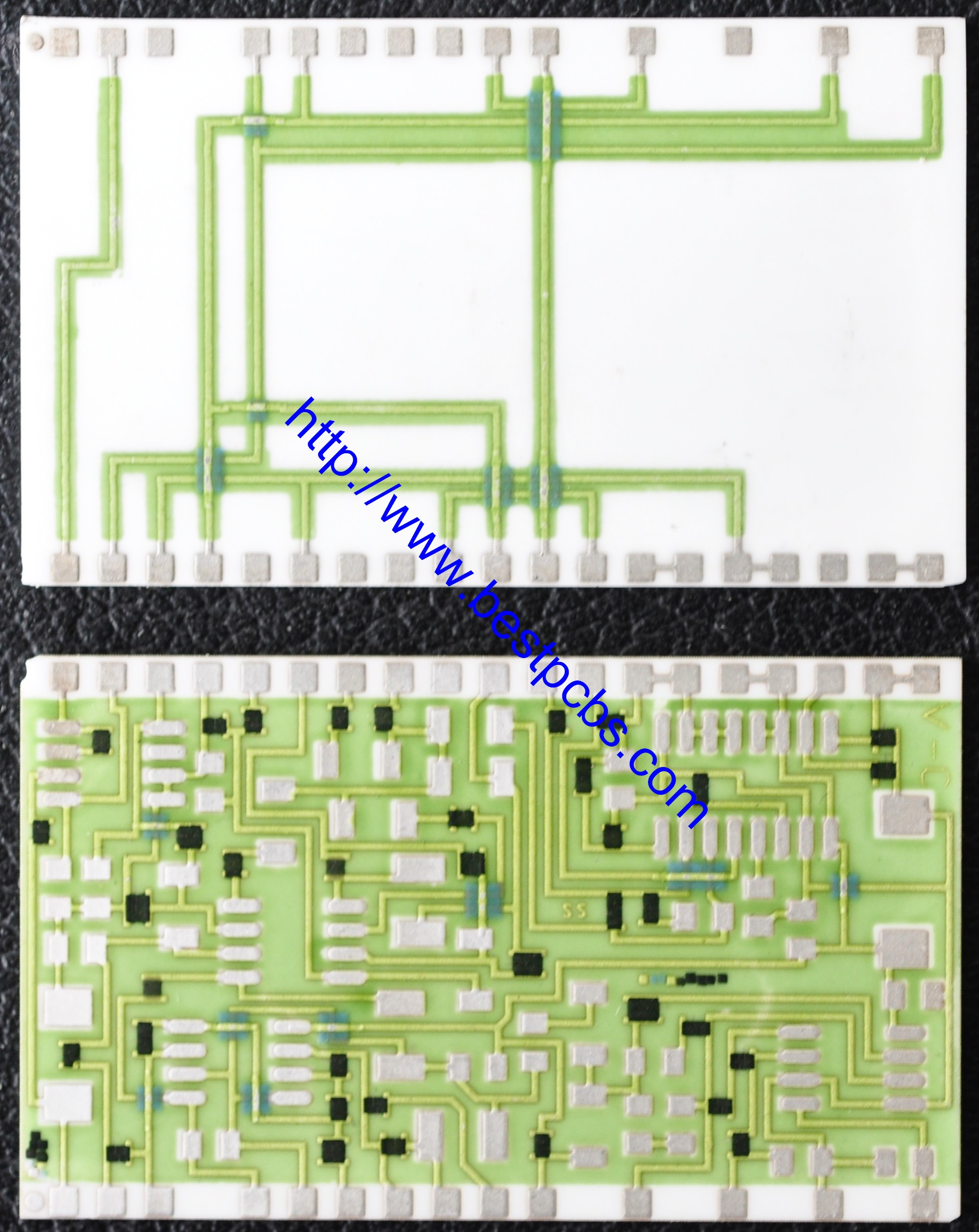
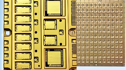
How Is Metallized Ceramic Substrate Manufactured?
Strict process control ensures consistent quality and performance in metallized ceramic substrate production.
Step-by-Step Manufacturing Flow
Ceramic blank preparation: Precision cutting, polishing, and deep cleaning
Surface activation: Enhances metal-ceramic bonding strength
Metallization: Sputtering, screen printing, or direct metal bonding
High-temperature sintering: Forms permanent, robust metal-ceramic bonds
Photolithography and etching: Defines precise circuit patterns
Plating: Ni/Au, Ni/Pd/Au for corrosion resistance and solderability
Final inspection: 100% testing of thermal resistance, adhesion, and dimensional accuracy
Where Is Metallized Ceramic Substrate Used in Medical, Aerospace & Industry?
Metallized ceramic substrate enables mission-critical performance across high-reliability industries.
Medical Application
MRI gradient coil power modules: AlN metallized ceramic substrate dissipates 500W+ of heat with zero signal interference, ensuring clear diagnostic imaging.
Aerospace Application
Satellite DC-DC converters: Withstands extreme temperature cycles (-40°C to 150°C) and cosmic radiation, delivering 10+ years of orbital reliability.
Industrial Application
IGBT inverter substrates: Si₃N₄ metallized ceramic substrate resists thermal shock from thousands of on/off cycles, eliminating factory downtime.
What Are Common Failures of Metallized Ceramic Substrate & Solutions?
Top Failures & Proven Fixes
Metal-ceramic delamination: Optimize surface activation and sintering parameters; use complimentary DFM analysis to avoid design-induced stress.
Insufficient thermal dissipation: Upgrade to AlN or Si₃N₄ material; optimize trace layout for maximum heat spreading.
Poor solderability: Apply uniform Ni/Au plating; control surface contamination during production.
Dimensional warpage: Use precision-ground ceramic blanks; balance metallization layer thickness across the substrate.
Why Choose EBestpcb as Your Metallized Ceramic Substrate Manufacturer?
For reliable, high-performance metallized ceramic substrate, EBestpcb is your top partner.
Fast lead times for prototypes and mass production
100% quality inspection with a zero-defect guarantee
Full industry certifications for medical, aerospace, and industrial compliance
Complimentary DFM analysis to optimize your design
Flexible MOQ for prototype sampling and dedicated technical support
What Services Do We Offer for Metallized Ceramic Substrate?
We provide end-to-end solutions for metallized ceramic substrate from design to finished parts.
Custom metallized ceramic substrate design and complimentary DFM review
Material selection support (Al₂O₃, AlN, Si₃N₄)
Precision metallization (sputtering, screen printing, direct bonding)
Plating services (ENIG, Ni/Au, Ni/Pd/Au)
Prototyping and mass production capabilities
Full reliability testing and quality validation
What Certifications Do We Hold for Metallized Ceramic Substrate Production?
Our certifications ensure global compliance and quality for metallized ceramic substrate.
ISO 9001: Quality management system certification
ISO 13485: Medical device manufacturing compliance
IATF 16949: Automotive quality standard
UL and RoHS certified for safety and environmental requirements
Aerospace material and process validation credentials
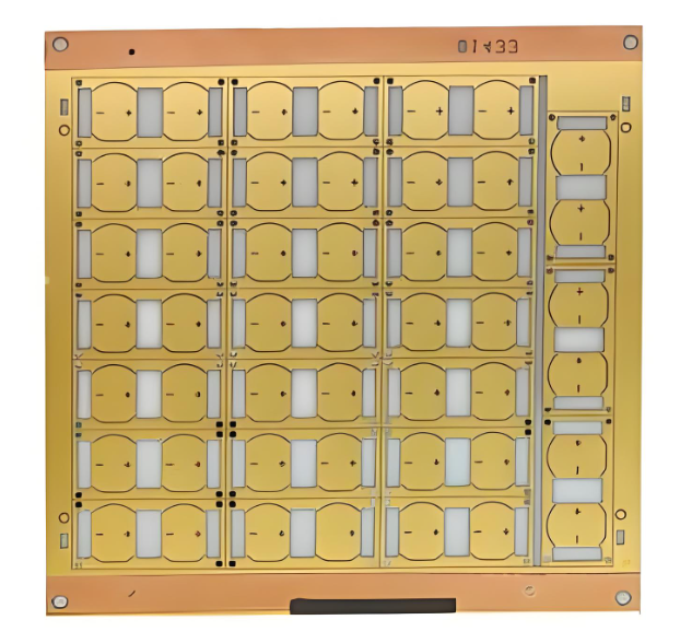
Our Metallized Ceramic Substrate Production Capabilities
Capability | Specification
Ceramic Materials | Al₂O₃ (96%/99%), AlN, Si₃N₄
Max Substrate Size | 200mm × 300mm
Thickness Range | 0.25mm – 5.0mm
Min Line Width/Space | 50μm / 50μm
Metallization Layers | Cu, Ni/Au, Ag/Pd
Plating Options | ENIG, Ni/Au, Ni/Pd/Au
Dimensional Tolerance | ±0.02mm
Thermal Conductivity | Up to 200 W/m·K (AlN)
Solve Your Toughest Metallized Ceramic Substrate Challenges—Partner With EBestpcb
Engineers and teams consistently face pain points with metallized ceramic substrate: thermal bottlenecks, delamination risks, inconsistent quality, long lead times, and lack of design support. We resolve these issues with optimized material selection, strict process control, complimentary DFM analysis, fast turnaround, and full compliance certifications. For mission-critical medical, aerospace, and industrial designs, trust EBestpcb for your metallized ceramic substrate needs—we deliver performance you can count on.
FAQ: Frequently Asked Questions About Metallized Ceramic Substrate
What is the best material for high-power metallized ceramic substrate?
Aluminum Nitride (AlN) is ideal, offering ultra-high thermal conductivity and thermal expansion that matches silicon chips.
How to prevent metallized ceramic substrate delamination?
Ensure proper surface activation, controlled sintering, balanced metal thickness, and complimentary DFM analysis before production.
What industries use metallized ceramic substrate most?
Medical devices, aerospace systems, industrial power electronics, automotive inverters, and laser equipment.
What is the difference between metallized ceramic substrate and thick film substrate?
Metallized ceramic substrate offers higher thermal conductivity and power handling, while thick film is cost-effective for low-power consumer electronics.
Can you customize metallized ceramic substrate for specific applications?
Yes—we provide custom materials, sizes, thicknesses, metallization, and plating for medical, aerospace, and industrial use cases.
What certifications do you hold for metallized ceramic substrate production?
We hold ISO 9001, ISO 13485, IATF 16949, UL, and RoHS certifications for full industry compliance.
How long is the lead time for metallized ceramic substrate prototypes?
Prototype lead times start at 7–10 days, with mass production timelines optimized for your volume requirements.
You may also like
Tags: aln ceramic substrate, ceramic substrate metallization, high power ceramic substrate, metallized ceramic substrate