

What is a ceramic RF PCB, and why do RF engineers choose it?
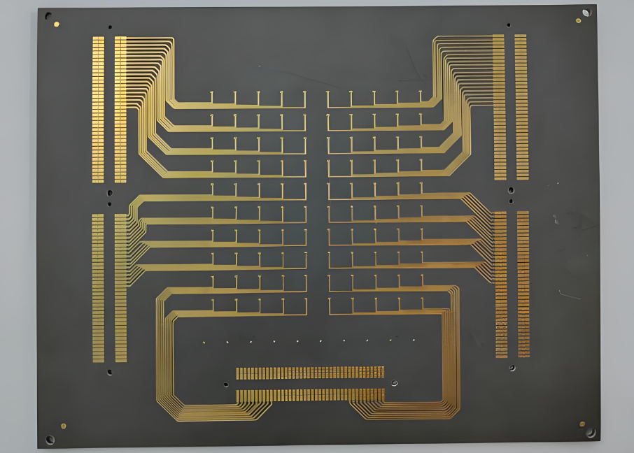
A ceramic RF PCB is a radio-frequency circuit board built on a ceramic substrate (most commonly alumina Al₂O₃ or aluminum nitride AlN) instead of woven-glass epoxy. A ceramic RF PCB is chosen when you need stable dielectric behavior, low RF loss, excellent heat spreading, and mechanical stiffness in a compact footprint.
In practical RF terms, ceramic substrates help when your design is sensitive to temperature drift, phase stability, or localized heating near power devices. They also make sense when you want a rigid platform for precision RF transitions, high-power RF matching networks, or compact modules where thermal and electrical margins are tight.
Quick definition in one minute
- Substrate: ceramic (Al₂O₃ or AlN) instead of FR-4 epoxy glass.
- Metallization: copper bonded or plated on ceramic (common routes include DPC/DBC/AMB).
- Typical goal: lower loss + better thermal control + more stable RF behavior.
Where ceramic RF boards outperform “ordinary” RF laminates
- Thermal headroom: ceramics spread heat far better than FR-4, keeping junction temperatures calmer under RF power.
- Parameter stability: Dk and mechanical dimensions tend to drift less with temperature and humidity than epoxy systems.
- Harsh environments: strong electrical insulation and high-temperature capability suit industrial and aerospace-style constraints.
Why choose EBest as your ceramic RF PCB manufacturer for prototypes and production?
If you are selecting a ceramic RF PCB manufacturer, you are not just buying a board. You are buying process control: metallization consistency, dimensional tolerance, RF-friendly fabrication choices, and assembly guidance that prevents expensive iteration.
EBest is positioned as a One-stop PCBA service provider, better understanding the needs of engineers. That matters because RF and ceramic projects often fail for “coordination” reasons, not theory reasons. Layout intent gets lost, stack-up assumptions shift, and the first build doesn’t match the simulation.
What engineers usually worry about
- RF loss and repeatability: controlled copper geometry, consistent process windows, and practical RF DFM checks.
- Thermal + reliability: substrate selection guidance, copper options, and assembly recommendations to reduce stress.
- Lead time risk: clear fabrication planning and rapid prototype-to-small-batch flow.
- Traceability: process tracking so you can debug issues with evidence, not guesses.
EBest advantages
- Free DFM, process adaptation suggestions
- 20 years, serving 1800+ customers, 10,000+ engineers
- One-Stop Service: PCB, Component, PCBA, Testing & Box-building
- NO MOQ, personal service
- ISO9001/13485, IATF16949, AS9100D
- MES & traceability
- 1.5-week rapid PCBA delivery (project-dependent)
- Technical support before & after sales
- Prototype & small volume welcome
- Quick turn-out, on-time delivery
- High quality, special request available
- Strong R&D team, know how-to
- Prompt feedback (within 12H)
When should you use a ceramic RF PCB instead of Rogers or FR-4?
Use ceramic when your RF design is being limited by temperature rise, phase drift, or tight spacing around hot devices. In contrast, use Rogers-like RF laminates when you need low loss in a standard PCB workflow and your thermal density is manageable. Use FR-4 when frequency is low enough and the design is tolerant to higher loss and wider variation.
Frequency, loss, and thermal triggers
- Thermal trigger: RF power devices or dense modules where FR-4 becomes a thermal bottleneck.
- Stability trigger: you care about phase stability across temperature or need consistent dielectric behavior.
- Packaging trigger: RF module integration, chip attach, or tight mechanical constraints.
Rules of thumb that work in real projects
- If your hotspot temperature is driving redesign, consider ceramic first.
- If you need “RF + power” in a compact module, ceramic often simplifies thermal design.
- If cost is the top constraint and frequency is modest, FR-4 can still be valid.
Ceramic RF PCB vs Rogers vs FR-4—what’s the real difference?
Here’s the practical comparison engineers use when deciding. Ceramic tends to win on thermal and stability. Rogers-type materials often win on mainstream RF PCB manufacturability. FR-4 wins on cost and availability.
| Factor | Ceramic RF PCB (Al₂O₃ / AlN) | Rogers-class RF laminates | FR-4 |
|---|---|---|---|
| RF loss (typical) | Low to very low (depends on ceramic + metallization) | Low (designed for RF/microwave) | Higher (loss rises quickly with frequency) |
| Thermal performance | Excellent (AlN especially strong) | Moderate (improves with fillers/stack choices) | Poor to moderate |
| Dielectric stability | High stability across temperature and humidity | Good stability (material-dependent) | More variable |
| Manufacturing ecosystem | More specialized (process and handling matter) | Mainstream RF PCB ecosystem | Most mainstream |
| Typical use cases | High-power RF modules, compact RF + thermal designs, harsh environments | Microwave/RF boards, antennas, RF front ends, 5G style designs | Low-frequency digital, cost-sensitive electronics |
| Cost level | Higher | Medium to high | Lowest |
Which ceramic substrate is best for RF—Alumina (Al₂O₃) or Aluminum Nitride (AlN)?
Choose alumina when you want a well-established, cost-effective ceramic substrate with good RF insulation and solid mechanical properties. Choose AlN when thermal conductivity is a primary driver and you want better CTE matching to certain semiconductor devices. Both can support RF work. The “best” depends on your power density and thermal budget.
| Property | Alumina (Al₂O₃) | Aluminum Nitride (AlN) | What it means for RF design |
|---|---|---|---|
| Dielectric constant (typ.) | ~9–10 (varies by grade/frequency) | ~8.5–9 (varies by grade/frequency) | Impacts line width for a target impedance and field confinement |
| Loss tangent (typ.) | Low (grade and frequency dependent) | Low (grade and frequency dependent) | Lower loss helps insertion loss and Q of matching networks |
| Thermal conductivity | Lower than AlN | High (commonly cited around 170 W/m·K for high-purity materials) | Matters when RF power creates hotspots and drift |
| Typical positioning | Balanced performance, broad use, cost-aware | Thermal-first, higher-end module designs | Pick based on power density and stability needs |
What are the main ceramic RF PCB metallization methods (DPC, DBC, AMB)?
Metallization is where many ceramic projects succeed or fail. The copper-to-ceramic interface affects adhesion, thermal cycling reliability, and even RF loss through surface quality and geometry control. In sourcing terms, you should ask which metallization route is used and why.
| Method | How it’s built | Strengths | Common RF + power use |
|---|---|---|---|
| DPC (Direct Plated Copper) | Copper is plated onto a prepared ceramic surface (often via thin-film seed + plating) | Fine features potential, good for density and pattern control | Compact RF modules, denser routing, controlled copper geometry |
| DBC (Direct Bonded Copper) | Thicker copper is directly bonded to ceramic at elevated temperature | Strong copper bond, good heat spreading, robust power handling | Power RF, heat-spreading bases, high current + RF hybrids |
| AMB (Active Metal Brazing) | Active braze layer bonds metal to ceramic | Strong bond options, suited for demanding mechanical/thermal cycling | Harsh environment modules and high reliability builds |
Which one should you pick?
- If you need finer geometry and dense routing, ask for DPC capability and design rules.
- If you need thick copper and strong heat spreading, DBC is a common go-to.
- If the environment is severe and reliability is the priority, discuss AMB tradeoffs early.
How do you design impedance on a ceramic RF PCB without guesswork?
Start with the “three numbers” that decide impedance: dielectric constant, dielectric thickness, and copper geometry. Then lock down the reference plane strategy. In ceramic RF work, small dimensional shifts can move impedance and phase, so you want a controlled stack definition rather than assumptions.
What to give your manufacturer
- Target impedance: 50 Ω, 75 Ω, or differential targets (state tolerance).
- Transmission line type: microstrip, stripline, or CPWG.
- Layer definition: dielectric thickness, copper thickness, and reference plane distance.
- Surface finish: ENIG, immersion silver, etc., because it can affect RF loss and solderability choices.
- Frequency band: so DFM can focus on what matters (loss vs geometry vs transitions).
Microstrip vs CPWG vs stripline on ceramic
- Microstrip: simple, easy probing, but more exposed fields.
- CPWG: excellent for grounding control and isolation when you add via fences.
- Stripline: best shielding, but stack and via transitions become more critical.
What layout rules reduce loss and improve isolation on ceramic RF PCB designs?
RF layout on ceramic rewards discipline. Keep return paths short, keep discontinuities intentional, and treat every transition like a component. The good news is ceramic’s rigidity helps keep geometry stable, which supports repeatability.
Ground strategy and via fences
- Put the ground plane close and continuous under RF traces.
- Use via fences along CPWG edges to reduce radiation and coupling.
- Maintain consistent via pitch near transitions and sensitive nodes.
Transitions (SMA, SMPM, chip-to-line)
- Model connector launches, then match pad geometry to your line structure.
- Keep component-to-line stubs short; use grounded coplanar transitions where possible.
- Define solder fillet targets for repeatable connector grounding.
Solder mask and surface finish choices
- For many RF structures, an exposed line (mask-open) can reduce dielectric variation.
- Pick finishes for both RF and assembly needs. Discuss silver vs ENIG tradeoffs early.
How do you handle assembly on ceramic RF boards to avoid cracks and low yield?
Assembly is where beginners get surprised. Ceramic is stiff and strong, but it does not behave like FR-4 under stress. The approach is simple: reduce mechanical shock, manage thermal gradients, and keep CTE mismatch in mind when placing large parts.
Paste, reflow profile, and fixture strategy
- Use fixtures that support the panel and reduce point loads.
- Use a controlled reflow profile to reduce rapid gradients across the substrate.
- For heavy parts, consider underfill or mechanical support if the use environment is harsh.
Component selection for ceramic (CTE + thermal cycling)
- Large ceramic packages and metal bodies can stress joints during cycling.
- Discuss critical components with your manufacturer so pad design supports reliability.
What tests prove a ceramic RF PCB is production-ready?
A good test plan covers both “board integrity” and “RF behavior.” You want to verify insulation, adhesion, and electrical continuity, then validate RF insertion loss and stability in the actual band that matters.
Electrical and physical verification
- Continuity / opens / shorts: baseline electrical test.
- Insulation resistance: supports high-reliability use.
- Adhesion check: verifies copper-to-ceramic robustness for thermal cycling.
RF validation that engineers trust
- S-parameters: insertion loss, return loss across band.
- Phase stability: compare across temperature points if your application is sensitive.
- Power test: verify heating, drift, and any arcing margins where applicable.
What affects ceramic RF PCB cost and lead time the most?
Cost and lead time are mainly driven by substrate choice, metallization route, feature density, and yield risk. If you want a faster, smoother first build, simplify what you can: keep via types practical, avoid unnecessary ultra-fine geometries, and design for panel efficiency.
The biggest cost drivers
- Substrate: AlN is typically more premium than alumina.
- Metallization: DPC/DBC/AMB choice changes process complexity.
- Geometry: fine lines, tight spacing, and special edge launches increase process control demand.
- Special requirements: thick copper, complex mechanical outlines, and custom tests add time.
How to cut cost without sacrificing RF performance
- Ask for DFM edits that keep impedance but relax non-critical tolerances.
- Use repeatable connector footprints and validated launch geometries.
- Plan a prototype step with RF coupons so production tuning is minimal.
FAQs
1. What frequency range is a ceramic RF PCB good for?
Ceramic substrates are commonly used when RF loss and stability matter, including microwave bands. The real limit is rarely the ceramic itself. It’s usually transitions, connector launches, and layout discipline. If you share your band and power level, the stack-up and line style can be tailored to your needs.
2. Is ceramic always better than Rogers for RF?
No. Ceramic is often better when heat and stability dominate. Rogers-class laminates are often better when you want low loss with a standard RF PCB workflow and lower total manufacturing complexity. The “right” choice depends on thermal density, mechanical constraints, and cost targets.
3. Should I choose alumina RF PCB or aluminum nitride RF PCB?
Choose alumina when you want a balanced, widely used ceramic with strong insulation and a more cost-aware path. Choose AlN when heat spreading is the main constraint and you want extra thermal margin. If you tell us your hotspot power and size, we can recommend the more efficient option.
4. What metallization should I use: DPC, DBC, or AMB?
DPC is attractive for finer geometry and density. DBC is common when you want thicker copper and heat spreading. AMB is often selected for demanding mechanical and thermal cycling conditions. The best answer comes from your copper thickness need, feature density, and reliability profile.
5. How do I specify controlled impedance for ceramic RF PCB fabrication?
Provide target impedance, line type (microstrip/CPWG/stripline), dielectric thickness, copper thickness, and the frequency band. Avoid assumptions. A controlled stack definition and an RF coupon strategy usually deliver the fastest path to a first-pass success.
6. Can EBest support ceramic RF PCB prototype builds and small volume production?
Yes. We welcome prototypes and small batches, and we can scale with you. You will also get engineering-facing feedback like Free DFM and process adaptation suggestions, so your early builds teach you something useful, not just consume budget.
7. What files do you need to quote a ceramic RF PCB and assembly?
Gerbers (or ODB++), stack-up notes, impedance targets, BOM (if assembly is needed), and any special test requirements are the usual starting point. If you already have a reference design or measured results, sharing that speeds up the review.
8. How do I submit an RFQ to EBest for ceramic RF PCB manufacturing?
Email your fabrication and assembly files with the target quantities, delivery expectation, and your application notes. The more you tell us about frequency, power, and operating temperature, the more accurate the DFM feedback and quotation will be.
Ready to build your ceramic RF PCB with an engineer-first team?
If you need ceramic RF PCB fabrication, ceramic RF PCB prototype support, or a full one-stop flow including components, PCB assembly, testing, and box-building, EBest can help you move from concept to verified hardware with fewer spins. Send your RFQ to sales@bestpcbs.com and tell us your frequency band, power level, and impedance targets so we can respond with practical DFM guidance and a build plan.