

If you are working on high-power electronics, LED lighting, or power conversion modules, thermal management is probably one of your biggest challenges. That’s where the double sided IMS PCB comes into play.
As a reliable IMS PCB manufacturer, EBest Circuit (Best Technology) has been helping engineers and purchasing teams solve complex design issues using double sided metal core solutions that offer excellent thermal performance and mechanical strength. Our products are widely used in various applications like LED lighting, automotive electronics, power modules, and more.
What Is a Double Sided IMS PCB?
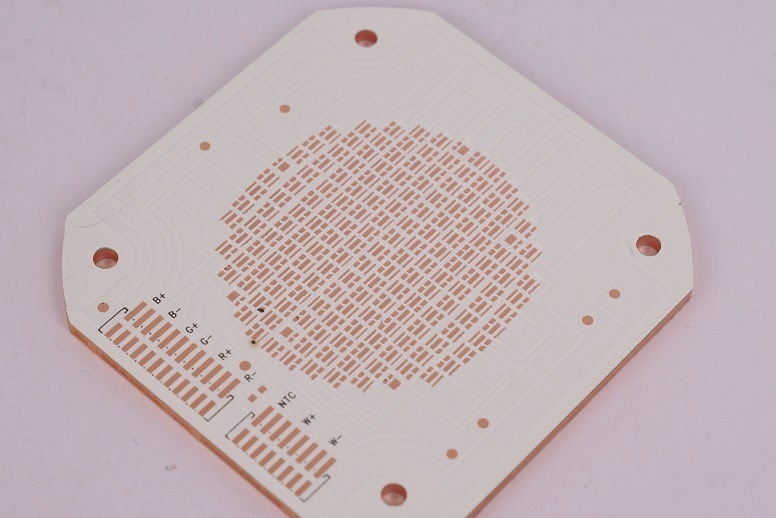
A double sided IMS PCB (Insulated Metal Substrate Printed Circuit Board) is a type of PCB that uses a metal base—typically aluminum or copper—combined with two copper layers and insulating dielectric layers in between. This structure allows designers to place components on both sides or route critical signals more efficiently while managing heat effectively.
Unlike single-sided IMS PCBs that have components and traces only on one side, double-sided versions support components mounting and traces layout both on top and bottom side, it allowed complex designs, higher current flow, and better heat transfer through thermal vias.
In simple terms: if your board gets hot and needs more routing space, a double sided IMS PCB can help.
Double Sided IMS PCB Structure
A double sided IMS PCB is built with multiple carefully selected layers, designed to balance electrical performance, mechanical strength, and heat dissipation. The general structure looks like this:
- Top copper layer: Carries the electrical traces and component pads.
- Top dielectric layer: An electrically insulating but thermally conductive material.
- Metal core: Usually aluminum or copper, it serves as a mechanical base and heat sink.
- Bottom dielectric layer: Same material as the top layer, separating the metal core from the bottom copper.
- Bottom copper layer: It is a trace layer, used for power, ground, or additional signal traces.
Plated through holes (vias) allow electrical connection between the top and bottom copper layers. These vias can also help conduct heat away from hot components into the metal core, improving thermal performance.
Types of IMS PCB Materials
In IMS PCB design, the metal base plays a critical role in heat dissipation and mechanical stability. The two most commonly used core materials are aluminum and copper, each with distinct advantages and application scenarios.
1. Aluminum-Based IMS PCB
Aluminum is by far the most widely used metal base material in IMS PCBs. It offers a great balance between cost, weight, and thermal performance. With a typical thermal conductivity of 1.0 to 3.0 W/m·K, aluminum is sufficient for most applications where moderate heat needs to be managed efficiently.
Advantages of aluminum base:
- Cost-effective: More affordable than copper, suitable for mass production.
- Lightweight: Ideal for weight-sensitive designs like automotive lighting and portable devices.
- Corrosion-resistant: Naturally forms a protective oxide layer, extending board life.
- Good thermal conductivity: Capable of dissipating heat from surface-mounted components quickly.
Typical applications:
- LED lighting systems (e.g. street lights, home bulbs)
- Power driver boards
- Consumer electronics
- Automotive LED modules
Aluminum IMS PCBs are perfect for designs that need reasonable thermal performance at a lower cost. They’re especially common in LED products, where keeping junction temperature low is essential to extending light source life.
2. Copper-Based IMS PCB
Copper-based IMS PCBs are chosen when thermal management becomes critical, or when mechanical robustness is equally important. Copper has a thermal conductivity of around 5.0 W/m·K—more than double that of aluminum—making it an ideal choice for high-power or high-density applications.
Advantages of copper base:
- Superior heat dissipation: Excellent for fast heat transfer in high-power designs.
- High mechanical strength: Less prone to flexing or warping under load or heat.
- Stable performance at high temperatures: Supports continuous operation in demanding environments.
- Better current carrying capacity: Enables narrower traces for the same current level.
Typical applications:
- Power inverters and converters
- Motor control units and industrial drives
- RF amplifiers and telecom power modules
- Aerospace and defense electronics
- High-performance LED arrays
Due to its higher cost and weight, copper is generally used in specialized applications where reliability, thermal performance, or current handling are mission-critical. It’s especially favored in automotive power systems, high-end industrial equipment, and aerospace control circuits.
Single vs Double Sided IMS PCB
When choosing between single-sided and double-sided IMS PCBs, understanding their structural and functional differences is essential. Below is a detailed comparison covering performance, design flexibility, manufacturing complexity, and cost.
| Comparison Aspect | Single Sided IMS PCB | Double Sided IMS PCB |
| Copper Layers | One layer on top | Two layers – top and bottom |
| Component Placement | Only on one side | Possible on both sides or top side with backside routing |
| Thermal Conductivity Path | Heat moves in one direction (top to base) | Heat can dissipate through both layers via thermal vias |
| Routing Flexibility | Limited routing options | More complex, denser routing possible |
| Via Usage | Usually no plated vias | Requires plated through vias for inter-layer connections |
| Design Complexity | Simpler, suitable for low-power applications | Supports more complex, high-current designs |
| Manufacturing Cost | Lower cost, fewer steps | Higher cost due to drilling, plating, and alignment |
| Board Thickness | Generally thinner | Slightly thicker due to multilayer structure |
| Current Carrying Capacity | Limited by single copper layer | Higher due to dual copper planes |
| Mechanical Strength | Moderate | Higher due to more balanced structure |
| Typical Applications | LED bulbs, indicator lights, basic power supplies | LED headlights, motor drivers, power inverters |
| Preferred Use Cases | Cost-sensitive and thermally moderate projects | Thermally demanding, high-power, or complex circuitry |
At EBest Circuit (Best Technology), we provide both types with full engineering support, helping you select the right option based on your performance goals and budget.
IMS PCB Design Considerations
Designing an effective IMS PCB, especially a double sided IMS PCB, requires more than just basic layout knowledge. As a professional IMS PCB manufacturer, we often find that early-stage design decisions directly impact not only the cost but also manufacturability, reliability, and thermal performance.
Here are our top recommendations to help you design a high-quality IMS PCB that meets both technical and production requirements:
1. Understand the Thermal Path Early
IMS PCBs are often chosen for their excellent heat dissipation. To maximize this advantage:
Place heat-generating components (like LEDs, power ICs, MOSFETs) directly above the metal core or near thermal vias.
- Use thermal reliefs for pads to balance solderability and heat transfer.
- Avoid thick dielectric layers if fast heat conduction is critical—choose higher thermal conductivity materials instead.
2. Use Plated Vias Wisely
In double sided IMS PCBs, plated through holes (vias) are crucial to connect the top and bottom copper layers. However:
- Vias increase cost due to drilling and plating steps.
- Avoid placing too many vias near mechanical mounting holes to prevent cracking during assembly.
- For high-current paths, increase via diameter and plating thickness, or use multiple thermal vias in parallel.
3. Optimize Trace Widths and Spacing
Due to higher currents in IMS boards:
- Use wider traces wherever possible, especially for power lines.
- Respect minimum clearance based on copper thickness and voltage—this prevents arcing and improves reliability.
- Avoid sharp 90° corners on high-current or RF traces; use 45° or curved corners instead.
If you’re not sure how wide your traces should be, send us your current ratings—we’ll recommend widths based on IPC standards and real-world performance.
4. Select Suitable Copper Thickness
For IMS PCBs, copper thickness directly impacts both electrical and thermal performance:
- Standard thickness is 1oz (35µm), suitable for low to medium current.
- For high current or improved thermal conduction, 2oz or 3oz copper is recommended.
- Very thick copper (up to 10oz) is possible, but it increases cost and etching complexity.
5. Component Layout Planning
- Avoid clustering hot components together—spread them out to help heat dissipation.
- Keep temperature-sensitive components (like ICs, sensors) away from heat sources.
- Leave clearance around mounting holes to prevent shorting with metal base.
6. Surface Finish Compatibility
Tell us your assembly process (manual, reflow, wave soldering) and component pitch—we’ll advise the best finish.
- ENIG is recommended for flat surfaces and fine-pitch components.
- HASL is affordable but not ideal for tight layouts.
- Immersion silver and OSP are good for high-frequency circuits.
7. Share Your Design Goals Early
Many designers only share Gerber files at the last step. But as a manufacturer, we can provide more value when we’re involved earlier.
- Let us know if your priority is cost, thermal performance, space saving, or high current.
- Share thermal simulation data if available—we can help validate materials and layout choices.
- If you’re unsure between aluminum and copper base, we can guide based on your budget and operating temperature.
Contact us early often helps reduce revisions, avoid design traps, and improve yield—saving both time and money.
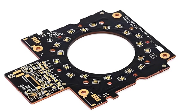
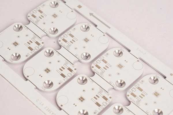
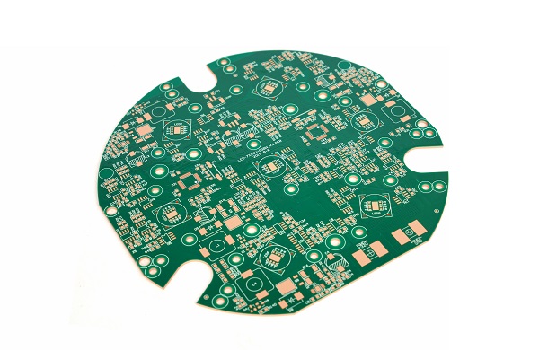
Double Sided IMS PCB Manufacturing Process
Manufacturing a double sided IMS PCB involves multiple controlled steps. Here’s we simply introduce the manufacturing processed involving in the insulated metal substrate fabrication:
1. Material Lamination
The copper foils and dielectric are laminated on both sides of the metal base with high pressure and temperature.
2. Drilling & Via Formation
Mechanical or laser drilling creates via holes through the board. These holes are then plated with copper to allow connectivity between top and bottom copper layers.
3. Imaging & Etching
Circuit patterns are created on both copper layers using photoresist and chemical etching.
4. Solder Mask Application
Solder mask is applied to protect copper from oxidation and to guide solder placement during assembly.
5. Surface Finishing
Finish is applied on copper pads to enhance solderability and prevent corrosion.
6. Testing
Electrical tests (shorts/opens) and inspection ensure product quality before packaging and shipment.
Here is a completed manufacturing process of IMS PCB.
Double Sided IMS PCB Surface Finish Options
- HASL (Lead-free): Affordable, but not ideal for fine-pitch components.
- ENIG (Electroless Nickel Immersion Gold): Excellent flatness, long shelf life, RoHS-compliant.
- ENEPIG: Very good solderability, corrosion resistance, durable.
- OSP: Cost-effective and environmentally friendly, but short shelf life.
- Immersion Silver: Good for high-frequency signals, flat and solderable.
- Hard Gold: Very durable, typically used for connectors or edge contacts, but rarely used in IMS PCB, it is popular in FR4 PCB.
At EBest Circuit (Best Technology), we recommend ENIG or ENEPIG for double sided IMS PCBs used in LED or power applications due to its durability and finish quality.
Cost Factors of Double Sided IMS PCB
The cost of a double sided IMS PCB is influenced by multiple variables, ranging from material selection to design complexity. As a manufacturer, we often find that many cost increases come from early design decisions. Here are the main cost drivers you should be aware of:
1. Material Type
Aluminum is more affordable and widely used, while copper offers better thermal performance but at a significantly higher price. If your project doesn’t demand extreme thermal performance, aluminum is usually the better choice from a budget perspective. High Tg costs more.
2. Copper Weight
Thicker copper layers allow for higher current carrying capacity and better heat dissipation, but they also increase cost:
- Standard: 1oz (35µm)
- Mid-range: 2oz – 3oz
- Heavy copper: 4oz – 10oz (used in power-intensive designs)
Heavier copper requires longer etching time and more material, which increases both processing time and price.
3. Board Size & Shape
Larger PCBs naturally use more material and occupy more space on the production panel. Irregular shapes also lead to more material waste and extra routing time.
- Square or rectangular boards make better use of panel space.
- Rounded or irregular outlines may require CNC routing or laser cutting, which adds cost.
4. Via Count and Type
Double sided IMS PCBs require plated through holes (PTH) to connect the two copper layers. The more vias you have, and the smaller their diameter, the more complex and expensive the drilling and plating process becomes. Via-in-pad, filled vias, and microvias are more expensive.
5. Dielectric Layer Thickness
Though not the focus here, it’s worth noting: if you select high-performance dielectric materials (e.g., with higher thermal conductivity or thinner thickness), the price will increase. These materials are more specialized and costlier to produce.
6. Special Features
Any additional processes will increase cost, such as:
- Via-in-pad or filled vias
- Selective plating or special coatings
- Edge plating or beveling
- Thermal simulations or FEA reports (optional support)
These are usually project-specific, so it’s best to clarify during the RFQ stage.
EBest Circuit (Best Technology) – Your Reliable IMS PCB Manufacturer
When it comes to manufacturing double sided IMS PCBs, experience, precision, and consistency matter. At EBest Circuit (Best Technology), we specialize in high-performance metal core PCBs tailored to thermal management, power conversion, and LED lighting applications.
We offer:
- Custom solutions using aluminum or copper base materials with various shapes
- Precision-controlled dielectric thicknesses for consistent thermal resistance
- Tight tolerance drilling and PTH plating for stable double-sided connections
- Surface finishes like ENIG, ENEPIG, OSP, and lead-free HASL to match your assembly needs
- Free DFM checks with technical support
- 24/7 before & after sales assist
- Professional sales can provide best solution tailored to your specific requirement
- Transparent price and data traceability
- High quality control followed IATF 16949
- No MOQ required, 1 pc available
Whether you need rapid prototypes or mass production, our engineering team supports you from design optimization to final testing. We believe that a good PCB starts with good communication—and we’re always ready to listen.
To get an accurate and cost-effective quote, always provide the following details upfront:
- Base material (Al or Cu)
- Copper thickness
- Board size and outline
- Layer count and via design
- Expected volume
- Surface finish
- Thermal performance requirements
Send your Gerber files or RFQ to sales@bestpcbs.com to get started.
FAQs
Q1: What is the thermal conductivity of a double sided IMS PCB?
It depends on the dielectric used. Standard ranges are 1.0 to 3.0 W/m·K, with higher options available for demanding designs.
Q2: Can I place components on both sides of a double sided IMS PCB?
Typically, one side is reserved for power routing or heat dissipation, but yes, it’s technically possible depending on the application.
Q3: What surface finish is best for LED applications?
ENIG is recommended for its flatness, solderability, and long shelf life.
Q4: Are double sided IMS PCBs expensive?
They cost more than single-sided IMS or standard FR4 PCBs, but offer much better thermal and electrical performance, especially for power-intensive designs.
Q5: How can I get a quote from EBest Circuit (Best Technology)?
Just email your Gerber files and requirements to sales@bestpcbs.com, and we’ll respond within 24 hours.