Looking for 2L aluminum base PCB prototyping solutions? This guide explores everything from material specs to cost-saving prototyping strategies for high-performance LED panel.
18 Years of Thermal Management Expertise – Your LED Panel’s Heat Dissipation Solved!
- Thermal Throttling? – Our “Heat Tunnel” via design drops junction temps by 40%
- Prototype Delays? – CAD-to-board in 24 hours with real-time DFM feedback
- Signal Noise? – Isolated power planes maintain 65dB EMI suppression
- Budget Constraints? – Standardized 300×400mm panels cut 12% tooling costs
Best Technology delivers:
- Precision Thermal Control – 2L aluminum base PCB with 8W/m·K conductivity prevents LED lumen decay under 85°C continuous operation
- Instant Prototyping – 24-hour rapid sampling with ±0.1mm drilling accuracy for design verification
- Cost-Smart Design – Panelization-ready layouts reduce 15% material waste vs. standard FR4
- Vibration Resistance – 1.5mm aluminum substrate withstands 20G mechanical shock in outdoor LED displays
Every 2L Aluminum base PCB – A Thermal Guardian for Brighter LED Performance! Welcome to contact us now: sales@bestpcbs.com.
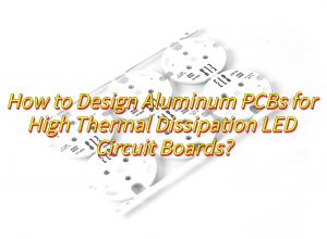
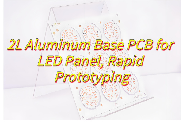
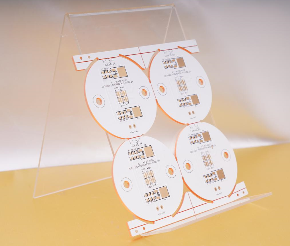
What Is 2L Aluminum Base PCB?
A 2L aluminum base PCB, also known as a double-layer aluminum substrate printed circuit board, is a specialized type of PCB designed for applications requiring efficient heat dissipation and mechanical stability. Unlike traditional PCBs, it features a layered structure with a conductive circuit layer bonded to an aluminum base, which acts as a heat sink to quickly transfer and disperse thermal energy.
This design makes 2L Aluminum Base PCBs particularly useful in high-power LED lighting, power converters, and automotive electronics, where managing excessive heat is essential for performance and longevity. The aluminum core not only enhances thermal conductivity but also provides structural rigidity, reducing warping under thermal stress. Additionally, the double-layer configuration allows for more complex circuitry while maintaining compact dimensions.
Due to their durability and thermal management capabilities, these PCBs are increasingly preferred in industries where reliability and heat resistance are priorities. Their construction typically includes a dielectric layer to ensure electrical insulation between the circuit and the metal base, balancing electrical functionality with thermal efficiency.
What Is Stackup Structure of 2L Aluminum Base PCB?
Below are the stackup structure of a 2L aluminum base PCB:
Top Copper Layer (Circuit Layer)
- Typically 1–4 oz copper foil thickness
- Contains etched conductive traces and component mounting pads
- Supports surface-mount device (SMD) assembly
Dielectric Insulation Layer
- Composed of thermally conductive polymer (e.g., polyimide or epoxy) with ceramic fillers
- Thickness ranges 0.003–0.006 inches (75–150 μm)
- Provides electrical isolation while enabling heat transfer
Aluminum Base Plate
- 0.5–3.0 mm thick aluminum alloy (usually 5052 or 6061 grade)
- Functions as primary heat spreader and mechanical support
- May include anodized surface treatment for corrosion resistance
Bottom Copper Layer (Optional Secondary Circuit Layer)
- Mirrors top layer capabilities when utilized
- Enables double-sided component placement or grounding planes
Protective Surface Finishes
- Top/bottom layers often feature HASL, ENIG, or OSP coatings
- Aluminum base may have insulating conformal coating
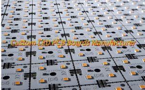
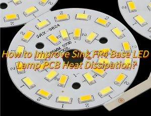
Why Choose 2L Aluminum Base PCB for LED Panel?
Here are reasons to choose 2L aluminum base PCBs for LED panel applications:
- Superior Heat Dissipation – The aluminum core efficiently transfers heat away from LED chips, preventing overheating and extending lifespan by maintaining stable operating temperatures.
- Enhanced Durability – Aluminum’s structural rigidity reduces warping under thermal cycling, ensuring long-term reliability in high-power or continuous-use LED installations.
- Improved Energy Efficiency – Effective thermal management minimizes energy loss due to heat buildup, optimizing LED brightness and power consumption.
- Compact Design Flexibility – The double-layer construction allows complex circuitry in a slim profile, enabling sleek, space-saving LED panel designs without compromising functionality.
- High Current Capacity – Thicker copper layers (up to 10 oz) support robust electrical pathways, ideal for high-intensity LEDs or densely packed arrays.
- Simplified Thermal Interface – Eliminates the need for additional heat sinks in many designs, reducing assembly steps and material costs.
- Consistent Light Output – Stable temperature control prevents luminance degradation over time, maintaining uniform brightness across the LED panel.
How to Choose the Right 2L Aluminum PCB Prototype Manufacturer for Your LED Panel?
Methods about how to choose the right 2L aluminum PCB prototype manufacturer for your LED panel:
Verify Thermal Management Specialization
- Confirm the manufacturer’s expertise in thermal simulation (e.g., ANSYS Icepak) for validating heat dissipation paths in your design. Request case studies demonstrating successful thermal solutions for LED arrays exceeding 100W. Ensure dielectric materials meet ≥1.5 W/mK thermal conductivity with UL 94 V-0 flame ratings.
Assess Aluminum-Specific Process Controls
- Require documentation of aluminum substrate pretreatment (chemical cleaning, anodization) to prevent delamination. Validate micro-etching techniques maintaining ≤3μm copper line precision and AOI systems detecting 15μm defects. Thermal shock testing protocols (-40°C to +150°C cycling) should be mandatory.
Evaluate Rapid Prototyping Capabilities
- Prioritize suppliers offering ≤72-hour prototype turnaround with live production tracking. Confirm readiness for engineering changes during fabrication without cost penalties. Small-batch capabilities (5-10 boards) with panelization efficiency ≥90% reduce material waste.
Scrutinize LED-Specific DFM Support
- Demand manufacturers provide design rule checks (DRC) for high-current traces (≥3A/mm²) and thermal pad optimization. Verify impedance control for mixed-signal designs and anti-caustic solder mask formulations resisting LED chemical exposure.
Confirm Multi-Stage Testing Protocols
- Ensure 100% electrical testing includes HV isolation (≥1500V AC/DC) between layers and aluminum base. Require thermal imaging reports showing ≤15°C hotspot differentials across LED clusters. Microsection analysis should validate dielectric thickness consistency (±10%).
Review Scalability Pathways
- Audit transition plans from prototypes to mid-volume production (1k-5k/month). Assess material inventory buffers for aluminum substrates and compatibility with automated SMT lines handling panel sizes ≥350×450mm.
Validate Supply Chain Transparency
- Require full material traceability including aluminum alloy grades (e.g., 5052/6061) and dielectric batch numbers. MES systems should provide real-time defect analytics and CPK data for critical parameters like copper thickness and insulation resistance.
How to Ensure 2L Aluminum PCB Prototype Fits Your LED Panel Design?
Ways to ensure 2L aluminum PCB prototype fits your LED panel design:
Validate Design Files Pre-Production
- Submit Gerber files, BOM, and assembly drawings to your manufacturer for a Design for Manufacturing (DFM) review. Confirm copper trace widths, via diameters, and solder mask layers align with the fabricator’s capabilities to avoid costly rework.
Match Material Specifications to LED Requirements
- Select aluminum substrate thickness (e.g., 1.5 mm for standard LED panels) and dielectric thermal conductivity (1.5–2.0 W/m·K) based on your LED’s power dissipation. Thicker copper layers (2 oz+) improve current handling for high-brightness LEDs.
Incorporate Thermal Vias and Pads Strategically
- Add thermal vias beneath LED footprints to enhance heat transfer to the aluminum base. Ensure via diameters and spacing comply with your manufacturer’s drilling limits to prevent misalignment during assembly.
Test Mechanical Fit Early
- Request a bare prototype board to verify mounting hole positions, panel cutouts, and edge clearances against your enclosure or heat sink. This prevents assembly delays caused by dimensional mismatches.
Simulate Thermal Performance Digitally
- Use thermal simulation tools to model heat flow from LEDs to the aluminum core. Compare results with real-world IR temperature testing on the prototype to refine dielectric layer thickness or copper weight.
Collaborate on Tolerance Stack-Up
- Work with your PCB supplier to define acceptable tolerances for board thickness, copper plating, and solder resist. Tighter tolerances (e.g., ±0.1 mm for board edges) ensure consistent alignment in multi-panel assemblies.
Perform Functional Testing Under Real Conditions
- Subject the prototype to accelerated aging tests at elevated temperatures (85°C+) and current loads matching your LED’s maximum rating. Monitor for solder joint fatigue or dielectric layer degradation before full-scale production.
How to Reduce the Cost of 2L Aluminum PCB Prototyping for LED Panels?
Maximize Panel Utilization via Array Nesting
- Action: Arrange multiple PCB designs on a single production panel (e.g., 8–12 small LED modules per 300mm×400mm panel).
- Cost Saved: Up to 40% on material costs by reducing scrap and optimizing aluminum substrate usage.
Standardize Material Specifications
- Action: Use common aluminum thicknesses (1.5mm) and dielectric layers (1.6mm prepreg, 1.5W/m·K thermal conductivity).
- Cost Saved: 15–20% through bulk purchasing discounts and shorter lead times.
Select HASL Surface Finish for Non-Critical Areas
- Action: Apply HASL to most of the board and reserve ENIG only for fine-pitch components.
- Cost Saved: 25–30% per unit by avoiding premium ENIG pricing (0.25–0.30/sq.in. vs. 0.10–0.15/sq.in. for HASL).
Early Design for Manufacturing (DFM) Collaboration
- Action: Engage your fabricator during layout design to fix issues like overly tight tolerances.
- Cost Saved: 30–50% on rework fees by eliminating errors before production (e.g., widening traces reduces etching scrap by 30%).
Order Prototypes in Small Batches for Volume Discounts
- Action: Request 5–10 units instead of 1–2 to qualify for tiered pricing.
- Cost Saved: 10–25% per unit
Reuse Modular Test Fixtures
- Action: Design adjustable jigs with interchangeable LED holders and thermal sensors.
- Cost Saved: 60–70% on test setup costs by avoiding custom fixtures for each design revision.
Adopt Open-Source Component Libraries
- Action: Use pre-certified LED footprints (e.g., KiCad’s 3535/5050 packages) instead of custom designs.
- Cost Saved: 40% on engineering time, saving 400–800 per project in labor costs.
How to Align 2L Aluminum PCB Prototypes with Your Fabrication Requirements?
Collaborate Early on Design for Manufacturability (DFM)
- Share your design files (Gerber, BOM, assembly drawings) with your fabricator before prototyping. They can flag issues like incompatible trace widths, insufficient solder mask clearances, or unrealistic tolerance demands. This reduces rework risks and ensures the design aligns with their machinery capabilities.
Specify Material and Thermal Performance Upfront
- Clearly define aluminum substrate thickness (e.g., 1.0mm, 1.5mm), dielectric thermal conductivity (1.0–3.0 W/m·K), and copper weight (1–3 oz). For example, high-power LEDs require 2.0 W/m·K dielectric to prevent overheating. Providing these specs upfront prevents delays from material substitutions.
Define Tolerances and Surface Finish Requirements
- Set acceptable tolerances for board thickness (±10%), hole diameters (±0.05mm), and copper plating (±10%). Choose surface finishes like HASL or ENIG based on your assembly process (e.g., wave soldering vs. reflow). Vague specs lead to mismatched prototypes and costly revisions.
Include Fabrication Notes for Special Features
- Highlight non-standard elements like countersunk holes, edge plating, or blind vias in your documentation. For instance, a note like “0.5mm depth countersink required for M3 screws” ensures manufacturers allocate the right tools and avoids errors during drilling.
Conduct Pre-Production Thermal Simulations
- Use software to model heat dissipation from LEDs to the aluminum base. Compare results with fabricator-provided dielectric specs. For example, a simulation might reveal that 1.5mm aluminum with 2.0 W/m·K dielectric keeps junctions below 90°C, validating your material choices.
Agree on Testing and Quality Assurance Protocols
- Define acceptance criteria like dielectric breakdown voltage (≥1.5kV DC), peel strength (≥1.4 N/mm), and solderability (per IPC-J-STD-003). Including these in your purchase order ensures prototypes meet reliability standards before shipment.
How to Improve the Efficiency of 2L Aluminum PCB Prototyping for LED Panels?
Automate Design Rule Checks (DRC) with DFM Software
- Use PCB design software (e.g., Altium, Eagle) with built-in DFM tools to auto-detect issues like trace spacing violations or incompatible hole sizes. This reduces manual review time by 50–70% and catches errors before fabrication.
Adopt Parallel Engineering for Design and Testing
- Begin thermal simulation and reliability testing planning while finalizing the PCB layout. For example, start sourcing thermal test chambers and drafting validation protocols during design iterations, shortening overall project timelines by 2–3 weeks.
Use Rapid Prototyping Technologies
- Prioritize laser-cut stencils and automated solder paste printers instead of manual stencils. Laser-cut stencils improve solder paste deposition accuracy by 30%, reducing rework from bridging or insufficient joints.
Implement Real-Time Collaboration Platforms
- Share 3D PCB models and thermal simulations with fabricators via cloud platforms (e.g., Onshape, Fusion 360). Real-time feedback loops cut communication delays by 40–60%, accelerating design iterations.
Leverage Pre-Certified LED Driver Circuit Libraries
- Use vendor-provided reference designs for LED drivers. These libraries reduce schematic entry time by 40% and ensure compliance with safety standards like UL or IEC.
Utilize Modular Test Fixtures with Quick-Change Inserts
- Design fixtures with magnetic or snap-fit inserts for different LED panel sizes. A modular system reduces setup time by 70% compared to custom fixtures, enabling faster functional testing across prototypes.
Prioritize In-House Thermal Imaging During Validation
- Invest in a low-cost thermal camera (500–1,000) to validate heat dissipation during early testing. Identifying hotspots in-house cuts reliance on external labs by 50%, accelerating design tweaks by 2–4 days per iteration.
Conclusion
This guide has explored the critical advantages of 2L Aluminum Base PCBs for LED panels, from their superior thermal management to cost-effective prototyping strategies. By understanding stackup design, material selection, and manufacturer alignment, you can optimize both performance and production efficiency. For reliable rapid prototyping with guaranteed thermal conductivity (≥2.0 W/m·K) and 24-hour turnaround options, contact Best Technology for a competitive quotation. Our expertise in LED-specific aluminum PCBs ensures your design transitions seamlessly from prototype to mass production. Request your customized quote today to accelerate your LED panel development timeline: sales@bestpcbs.com.