Seeking for in house PCB prototyping solutions? Discover how in-house PCB prototyping accelerates your design cycle while ensuring quality control. This guide covers prototyping benefits, manufacturing processes, and smart selection criteria.
Best Technology delivers fast, reliable PCB manufacturing to keep your projects on track. When time is critical, our 24-hour rapid prototyping (including 4-6 layers boards) helps you meet tight deadlines without compromising quality. We provide transparent pricing and no hidden fees for tooling, shipping, or design changes, so you can budget with confidence. Our free design reviews identify potential issues early, preventing costly delays, while real-time production tracking keeps you informed at every step. For growing businesses, we offer bulk-order savings and a proven 99.2% on-time delivery rate since 2020. Startups benefit from reduced engineering costs (up to 40%) thanks to our on-site material inventory (FR-4 to Rogers 4350B) and secure IP protection. Whether you need 1-10 prototypes or 10,000+ units, we maintain consistent quality with triple inspections (AOI, flying probe, impedance testing). Partner with us to simplify PCB manufacturing now: sales@bestpcbs.com.
What Is In House PCB Prototyping?
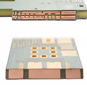
In house PCB prototyping describes the practice of developing and producing printed circuit board samples entirely within a company’s own manufacturing facility. This self-contained approach enables engineers to execute the complete PCB prototyping process from design validation and material selection to etching, drilling, and assembly without relying on external partners. In house PCB prototyping provides immediate access to production equipment like solder paste printers and pick-and-place machines, allowing for rapid design iterations and real-time process adjustments. The method proves particularly effective when handling proprietary designs, urgent project timelines, or experimental technologies that require controlled development environments. Organizations implementing in house PCB prototyping typically maintain dedicated cleanrooms, testing stations, and skilled personnel to ensure prototype accuracy while preserving intellectual property throughout the development cycle.
Why In House PCB Prototyping?
Here are reasons why choose in house PCB prototyping:
- Eliminate Vendor Delays – External PCB shops often take days or weeks for prototype delivery. With In House PCB Prototyping, you cut waiting times from weeks to hours, accelerating product development.
- Avoid Costly Design Revisions – When outsourcing, small errors require resubmitting files and paying again. In House PCB Prototyping lets you tweak designs instantly, saving both time and money.
- Protect Confidential Designs – Third-party vendors pose IP risks. In House PCB Prototyping keeps sensitive circuit layouts secure within your facility.
- Solve Problems in Real Time – If a prototype fails, engineers can inspect, adjust, and rerun production immediately instead of waiting for external feedback.
- Test Unconventional Materials – External shops may reject experimental substrates. In House PCB Prototyping allows testing specialized materials without restrictions.
- Reduce Small Batch Costs – Outsourcing low-volume prototypes is expensive. In House PCB Prototyping makes small runs economical by eliminating vendor markups.
- Maintain Supply Chain Stability – External shortages won’t disrupt your schedule when you control production internally.
- Customize Assembly Processes – Some designs need unique soldering or stacking methods. In House PCB Prototyping enables process adjustments without vendor limitations.
- Accelerate Debugging – On-site prototyping means faster signal testing, thermal validation, and mechanical fit checks.
- Scale Faster to Mass Production – Well-optimized In House PCB Prototypes transition smoothly to volume manufacturing with fewer surprises.
What Are Applications of In House PCB Prototyping?
Here are the practical applications of In House PCB Prototyping, addressing real industry needs and customer challenges:
- R&D Labs & Universities – Research teams use in house PCB prototyping to test experimental circuit designs quickly, avoiding long vendor lead times that slow down innovation.
- Medical Device Development – Medical prototypes often require strict compliance checks. In house PCB prototyping allows iterative testing to meet regulatory standards faster.
- Aerospace & Defense – Sensitive military-grade electronics demand confidentiality. In house PCB prototyping prevents external exposure of classified designs.
- Automotive Electronics – EV and ADAS systems need rapid hardware validation. In house PCB prototyping enables quick iterations for thermal and signal integrity testing.
- Industrial Automation – Custom control boards for machinery need robustness testing. In house PCB prototyping accelerates failure analysis and improvements.
- Consumer Electronics – Startups use In House PCB Prototyping to refine product features without waiting for external suppliers, speeding time-to-market.
- High-Frequency RF Designs – 5G and radar systems require precise impedance control. In house PCB prototyping allows immediate adjustments to meet performance targets.
- Low-Volume Custom Orders – Niche products with small batches benefit from in house PCB prototyping, avoiding high external prototyping costs.
How to Achieve In House Rapid PCB Prototyping?
- Equip with Agile Hardware: Use compact CNC machines, laser imagers, and auto-solder printers for fast setup between projects. Self-calibrating tools reduce human error.
- Automate Design Handoff: Link EDA tools to in-house CAM software for instant Gerber validation and toolpath generation. Engineers submit designs directly to production queues.
- Stock Essential Materials: Maintain FR-4, solder masks, and finishes (HASL/ENIG) on-site. Smart inventory systems track usage and partner with local suppliers for 24-hour replenishment.
- Cross-Train Teams: Certify staff to operate multiple machines and enforce DFM rules during design. Weekly sessions resolve recurring issues (e.g., trace spacing errors).
- Accelerate Testing: Use flying probe testers and AOI for immediate electrical/solder checks. Share digital results to cut revision cycles by 50%.
- Adopt Cloud Collaboration: Secure platforms enable real-time design reviews and version control, preventing outdated files from entering production.
- Run 24/7 with Energy Efficiency: IoT-monitored machines and UPS systems allow overnight production. Night shifts cut lead times without overtime costs.
- Offer Tiered Service Levels: Charge by material/machine hours for “Express” (24hrs) or “Priority” (48hrs) options. Clients balance speed and budget transparently.
- Reuse Proven Templates: Build a searchable library of past projects (stack-ups, impedance controls). AI tools help engineers retrieve data faster.
- Highlight Cost Metrics: Report 40–60% savings vs. outsourcing (lower per-unit costs, no expedited fees) and 50% faster time-to-market.
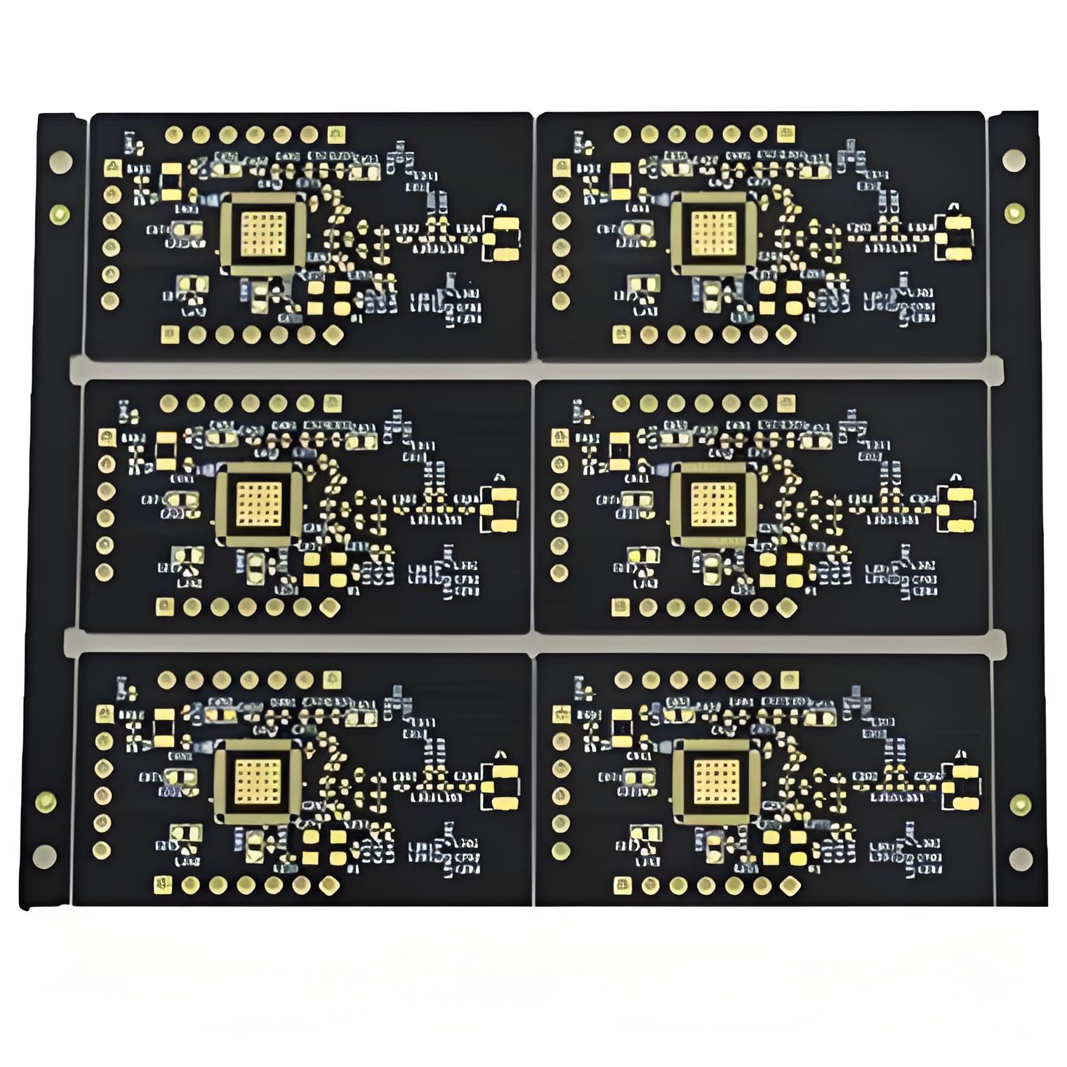
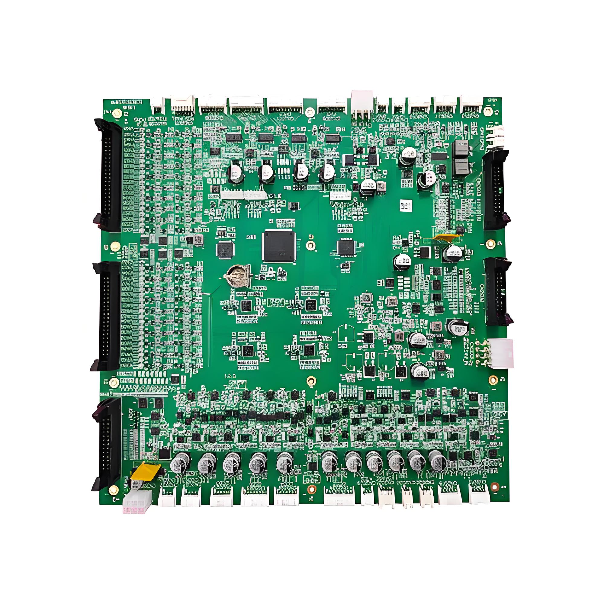
What Is In House PCB Manufacturing?
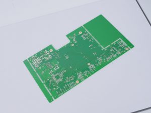
In house PCB manufacturing means making circuit boards entirely within a company’s own facility instead of using outside suppliers. This gives engineers full control over the entire process – from design and fabrication to assembly and testing. By keeping production on-site, companies can make boards faster (often in days instead of weeks), protect sensitive designs, and easily make changes during development. The process uses specialized equipment like milling machines, etching systems, and testing tools all located in the company’s workspace. While setting up requires investment in equipment and training, it helps avoid supply chain problems, lowers costs for prototypes, and allows work on special board designs that outside manufacturers might not handle. This approach works well for research projects, small production runs, and designs that need frequent changes, as engineers can quickly test and adjust boards as they’re being made.
How to Identify An In House PCB Manufacturer?
Below are methods about how to identify an in house PCB manufacturer:
- Ask for a Facility Walkthrough: Request a video or live tour showing their production floor. In House PCB Manufacturers will display etching lines, drilling machines, and assembly stations operating under one roof, eliminating outsourcing delays.
- Test Their Response Speed: Submit a minor design change and track revision time. True In House PCB Manufacturers often deliver updated prototypes within 24–48 hours since production is managed internally.
- Request Internal Testing Reports: Ask for inspection records (e.g., impedance tests, thermal imaging). In House PCB Manufacturers provide detailed logs from their own labs instead of third-party certifications.
- Evaluate Material Transparency: Inquire about laminate suppliers or copper sourcing. Manufacturers handling raw materials directly (e.g., stocking FR4 or ceramic substrates) typically offer better cost control and traceability.
- Propose a Custom Requirement: Submit an unconventional request (e.g., odd board shapes or mixed materials). In House PCB Manufacturers adapt quickly because their engineers work alongside production teams.
- Verify Data Security Practices: Check how design files are stored. Look for on-premises servers or isolated networks—common in In House PCB Manufacturers to prevent external data leaks.
- Demand Live Production Evidence: Request real-time footage of their production line in action. Authentic In House PCB Manufacturers can showcase raw material handling → etching → drilling → testing processes without cutaway transitions.
- Challenge With Tight Deadlines: Place a small test order with aggressive timelines (e.g., 3-day prototype). In House PCB Manufacturers typically meet urgent requests more consistently since they control the entire workflow.
What Are Processes of In House PCB Manufacturing?
Here’s a detailed breakdown of In House PCB Manufacturing processes, written with practical clarity from a customer’s perspective:
1. Design File Review and Engineering Feedback: Your PCB design files (Gerber, drill files) are analyzed by manufacturing engineers working in the same facility. In House PCB Manufacturing allows direct communication between designers and production teams to resolve issues before fabrication begins.
2. Material Selection and Preparation: Copper-clad laminates are cut to required sizes from bulk sheets stored in the facility’s material warehouse. In House PCB Manufacturing maintains material inventory under controlled conditions to prevent moisture absorption or contamination.
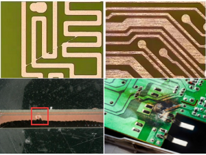
3. Inner Layer Processing: Dry film resist is laminated onto copper layers, exposed with your circuit pattern using laser direct imaging (LDI), then developed and etched. In House PCB Manufacturing performs this process in cleanroom conditions with automated optical inspection (AOI) after etching.
4. Oxide Treatment and Layer Stack-up: Inner layers undergo chemical oxidation to improve bonding. Layers are precisely aligned using optical targets and stacked with prepreg bonding sheets. In House PCB Manufacturing uses hydraulic presses with temperature profiling for consistent lamination.
5. Mechanical Drilling: CNC drilling machines create holes for vias and component leads based on your drill files. In House PCB Manufacturing performs drill bit changes and diameter verification in-house, maintaining tight hole position tolerances.
6. Electroless Copper Deposition: Drilled panels go through desmear and electroless copper plating to make hole walls conductive. In House PCB Manufacturing controls plating bath chemistry and temperature continuously for uniform copper thickness.
7. Outer Layer Imaging and Pattern Plating: Outer layers receive photoresist application, exposure, and development similar to inner layers. Additional copper is electroplated onto traces, followed by tin plating as etch resist. In House PCB Manufacturing adjusts plating currents for different board areas.
8. Etching and Strip Processes: Unwanted copper is chemically removed, leaving only tin-protected circuit traces. The tin is then stripped away. In House PCB Manufacturing monitors etch rates and solution concentrations in real-time.
9. Solder Mask Application: Liquid photo-imageable solder mask is applied, exposed through your solder mask artwork, and developed. In House PCB Manufacturing performs multiple curing stages with precise temperature control.
10. Surface Finish Application: Your chosen surface finish (HASL, ENIG, OSP, etc.) is applied using dedicated equipment. In House PCB Manufacturing maintains separate lines for different finishes to prevent cross-contamination.
11. Silkscreen Printing: Component markings and logos are printed using screen printing or inkjet methods. In House PCB Manufacturing verifies legibility and alignment against your documentation.
12. Electrical Testing: Flying probe or fixture testing checks continuity and isolation according to your netlist. In House PCB Manufacturing can immediately retest and troubleshoot failing boards.
13. Final Inspection and Packaging: AOI machines and manual inspectors verify dimensions, appearance, and functionality. In House PCB Manufacturing packages boards with appropriate anti-static materials and protective spacing.
Differences Between In-House vs Out-House PCB Manufacturing
Here’s a comprehensive comparison between In-House and Out-House PCB Manufacturing, written from a customer’s perspective with detailed, practical distinctions:
- Production Control & Adjustments
In-House: Immediate adjustments possible during manufacturing. Engineers can modify processes in real time if issues occur.
Out-House: Changes require communication with external vendors, often causing delays in implementation. - Lead Time & Delivery Speed
In-House: Shorter turnaround since all processes occur in one location without shipping delays between stages.
Out-House: Additional time needed for transport between different suppliers, extending delivery schedules. - Quality Assurance & Consistency
In-House: Direct monitoring of each step ensures uniform quality. Defects are caught and corrected early.
Out-House: Quality depends on the external manufacturer’s standards, which may vary between batches. - Communication Efficiency
In-House: Designers and production teams collaborate directly, enabling quick problem-solving.
Out-House: Miscommunication risks increase when multiple parties are involved, potentially delaying resolutions. - Cost & Pricing Structure
In-House: Lower costs for high-volume production due to reduced outsourcing fees and bulk material purchasing.
Out-House: May offer competitive pricing for large orders but often includes markup fees for smaller batches. - Customization & Flexibility
In-House: Easier to accommodate last-minute changes, special materials, or unique design requests.
Out-House: Limited flexibility once production begins, as external manufacturers follow fixed schedules. - Intellectual Property & Confidentiality
In-House: Designs remain within one facility, reducing the risk of leaks or unauthorized sharing.
Out-House: Requires sharing proprietary files with third parties, increasing security concerns. - Scalability & Production Capacity
In-House: Best for stable, predictable production volumes with controlled capacity.
Out-House: Can leverage multiple suppliers to handle sudden demand spikes more easily.
Conclusion
In conclusion, that’s all about prototyping benefits, manufacturing processes, and smart selection criteria. If you have any other issues about in house PCB prototyping and manufacturing, welcome to contact us at: sales@bestpcbs.com.