
Looking for single layer PCBs solution? Discover its definition, benefits, usage, why choose Best Technology as a PCB partner and design tips.
What Is Single Layer PCBs?
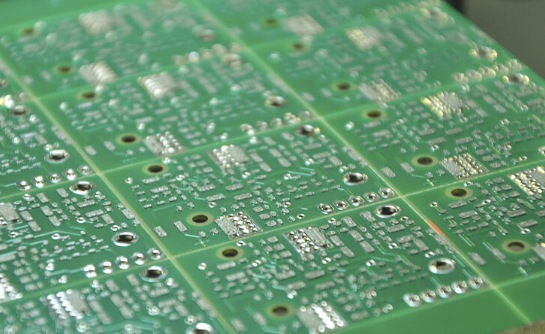
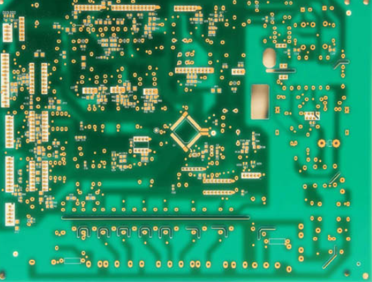
Single layer PCBs are fundamental and classic members of the PCB family, occupying an irreplaceable position in the field of electronics manufacturing. Through processes such as copper foil etching and drilling on a single side of an insulating substrate, the originally flat copper foil is transformed into a precise conductive circuit network, ultimately enabling stable electrical connections between electronic components. Characterized by their simple structure and controllable costs, these circuit boards serve as the ideal circuit carriers for entry-level electronic products such as calculators, simple remote controls, and toy circuits. For electronics engineers, single-layer PCBs are not only educational tools for learning circuit design but also efficient means for validating ideas and rapid prototyping. In mass production, single-layer PCBs significantly reduce production costs and lead times due to their ease of manufacturing, making them the preferred solution for cost-sensitive consumer electronics.

Advantages of Single Layer PCBs
- Significant Cost Advantage: Compared with multi-layer boards, single-layer printed circuit boards (Single Layer PCBs) do not require complex manufacturing processes such as interlayer lamination and blind/buried via processing. This significantly reduces raw material procurement costs and production processing expenses, demonstrating extremely high cost-effectiveness in projects with strict cost control requirements.
- Efficient Production Cycle: Due to the streamlined process flow, the cycle from design finalization to product delivery for single-layer printed circuit boards is greatly shortened. This efficiency enables it to quickly respond to urgent order demands and shows significant time cost advantages in small-batch trial production scenarios.
- Excellent Maintainability: The characteristic of having the circuit layout concentrated on a single layer makes the fault diagnosis and repair process more intuitive. With a clear circuit topology, technicians can quickly locate fault points and complete repair work efficiently, greatly improving the convenience and efficiency of post-maintenance.
- Flexible Design Adaptability: Single-layer PCB design does not need to consider complex issues such as interlayer signal interference and stack-up planning, allowing engineers to adjust the circuit layout more freely. For electronic devices with simple structures and clear functions, personalized design solutions can be quickly implemented, effectively reducing the design threshold and iteration costs.
- Superior Heat Dissipation Performance: The circuit traces of single-layer boards are distributed on the same plane, reducing the obstruction of interlayer insulating materials, enabling heat to be conducted more directly through the metal traces to the heat dissipation area. In low-power devices with non-extreme heat dissipation requirements, single-layer PCBs can achieve efficient natural heat dissipation by optimizing trace width and copper pour area.
- Wide Compatibility: Single-layer printed circuit boards meet the requirements of various standard packaging and soldering processes, and are seamlessly compatible with mainstream components such as through-hole technology (THT) and surface mount technology (SMT). Whether it is the upgrading and transformation of traditional electronic devices or the rapid verification of emerging applications, its high compatibility ensures the stable operation of the system.
The Uses of Single Layer PCBs
- Consumer electronics field: single-layer boards are commonly used in basic control circuits of simple remote controls, electronic toys, etc.
- Industrial control scenarios: single-layer boards are mostly adopted for small sensors and relay control boards to achieve signal transmission and control functions.
- Automotive electronics: some auxiliary circuits, such as in-vehicle lighting control modules, use single-layer boards to reduce costs and design complexity.
- Basic communication equipment modules: like the power management boards of simple routers, single-layer boards are often used as the hardware carriers.
- Smart home devices: low-cost door and window sensors, simple thermostats, etc., rely on single-layer boards to complete circuit design.
- Office automation equipment: the simple control panels of printers and the basic signal processing boards of scanners also choose single-layer boards.
- Medical equipment: some auxiliary circuits of basic monitors, as well as low-cost home health detection devices, also widely use single-layer boards for circuit construction.
Our Service For Single Layer PCBs
We offer a one-stop, full-process closed-loop service system for single layer PCBs, ensuring seamless integration from conceptual design to final product delivery:
- Customized Design: Relying on our team of experienced engineers and leveraging professional design tools such as Altium Designer and Eagle, we provide schematic drawing, PCB layout design, DFM (Design for Manufacturability) optimization, and other services. These are tailored to meet customers’ circuit functionality requirements, installation size constraints, and cost budgets, ensuring that the design solutions are both functional and production-feasible.
- Rapid Prototyping Service: Equipped with advanced PCB prototyping equipment, we support 24-hour urgent prototyping. Using high-precision laser cutting and chemical etching processes, and strictly controlling hole diameter accuracy and line width/line spacing tolerances, we can deliver samples in as fast as 3 working days, enabling customers to quickly validate their product designs.
- Large-scale Mass Production: Our standardized production workshop is outfitted with fully automated SMT placement lines and AOI optical inspection equipment, with a monthly production capacity exceeding 100,000 square meters. Certified by the ISO 9001 quality management system, we ensure that every single layer PCB passes rigorous testing, including high/low-temperature testing and withstand voltage testing, meeting the mass production needs of various industries such as communications, consumer electronics, and industrial control.
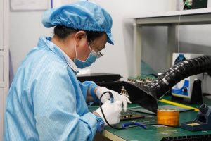
- Professional Assembly Services: We provide integrated services covering component procurement, surface mount soldering, through-hole assembly, and finished product testing. With long-term partnerships with internationally renowned component suppliers, we guarantee material quality. We use X-RAY inspection technology for solder joint quality analysis, and the final products undergo a 72-hour burn-in test to ensure long-term stable operation. Whether it’s validating the conceptual design of an innovative product or mass-producing a mature solution, we can provide high-quality and reliable single layer PCB solutions with outstanding technical capabilities and efficient response times.
Our Capability For Single Layer PCBs
| Item | Parameter Details |
| Minimum line width / line spacing | Achieve a fine routing process of 5 mil / 5 mil to meet the requirements of high density circuit design and ensure the stability of signal transmission. |
| Smallest Pore Size | Achieve precise control over minimum aperture size down to 0.3mm through advanced drilling technology, ensuring smooth bore walls and high dimensional accuracy to accommodate diverse component installations. |
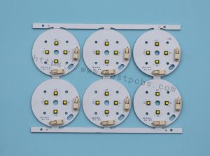
| Type of Board | It supports a variety of circuit boards such as FR – 4, CEM – 1, and aluminum substrates. Among them, FR – 4 circuit boards have good electrical properties and mechanical strength; CEM – 1 offers high cost – effectiveness; aluminum substrates have excellent heat dissipation performance. You can flexibly choose according to different application scenarios. |
| Maximum Plate Size | The maximum processing board size can reach 600mm × 1000mm, meeting the design requirements of large single-sided boards and being suitable for fields such as industrial control and communication equipment. |
| Surface Treatment | We offer a variety of surface finishing processes, including hot air solder leveling (HASL), immersion gold plating, and organic solderability preservative (OSP). The hot air solder leveling process can enhance solderability; immersion gold plating features excellent oxidation resistance and flatness; OSP treatment can effectively protect the copper surface, ensuring reliable soldering. |
Why Choose Best Technology As Your Single Layer PCB Manufacturer?
This is why choose Best Technology as your single layer PCB manufacturer:
- Competitive Price: We are committed to offering high-quality PCB solutions at competitive prices. By optimizing our production processes and managing costs efficiently, we ensure that you get the best value for your investment.
- Quality Guarantee: At Best Technology, quality is our top priority. We perform strict quality control procedures cover every stage of production, from raw material selection, prototyping to final product testing.
- Turnkey Service: Our all-in-one approach simplifies supply chain, shorten lead times, and improves communication efficiency. And we have one-on-one sales-assistant service to give you a wonderful experience work with us.
- On-Time Delivery: We understand the importance of meeting your project deadlines, and we offer online WIP updates to make sure you can keep track of the progress of your PCB product.
- Rapid Prototyping: We support 24 hours rapid prototyping for urgent orders.

The Manufacturing Process of Single Layer PCBs
Below is a simple introduction of single layer PCBs manufacturing process:
Step 1: Design File Review
- Conduct a thorough inspection of the customer-provided Gerber files, verifying accuracy of circuit traces, aperture sizes, and other critical parameters.
Step 2: Material Cutting
- Precisely cut insulating substrate materials to specified dimensions according to the design blueprint.
Step 3: Drilling
- Create precise component mounting holes and via holes at designated locations using CNC drilling equipment.
Step 4: Pattern Transfer
- Transfer circuit patterns onto the copper foil surface through photolithography processes including exposure and development.
Step 5: Etching
- Employ chemical etching to remove excess copper, leaving only the intended circuit patterns intact.
Step 6: Surface Finish Application
- Apply protective coatings such as HASL (Hot Air Solder Leveling) or ENIG (Electroless Nickel Immersion Gold) to enhance solderability and corrosion resistance.
Step 7: Profiling
- Cut the fabricated boards into final assembly shapes using CNC routing or V-scoring techniques.
Step 8: Quality Inspection
- Perform comprehensive quality checks including flying probe testing and visual inspection to ensure compliance with specifications.
Single Layer PCBs Design Consideration
- Plan Component Layout Rationally: When designing single-layer PCBs, start by arranging components according to the principle of “large before small, difficult before easy.” Ensure proper spacing between components to facilitate installation and heat dissipation.
- Avoid Long Parallel Traces: During the routing process, steer clear of long-distance parallel traces to prevent signal interference. Parallel paths can act as antennas, picking up and transmitting unwanted noise.
- Prioritize Critical Signal Integrity: Give precedence to maintaining the integrity of key signal lines. Use shorter, direct routes and consider impedance matching for sensitive signals to minimize signal degradation.
- Incorporate Sufficient Test Points: Strategically place test points throughout the PCB layout. These points are essential for post-production debugging, electrical testing, and quality assurance.
- Optimize for Manufacturing: Design with the manufacturing process in mind. Account for the limitations of single-layer PCB fabrication, such as potential trace density constraints and via requirements.
- Manage Power and Ground Traces: Route power and ground traces to provide stable electrical supply. Create wide, continuous paths to reduce resistance and ensure efficient current flow.
- Verify Design Rules: Before finalizing the design, thoroughly check against PCB design rules, including minimum trace width, clearance requirements, and mechanical constraints.
What Problems Can Single Layer PCBs Solve?
- Cost control: By simplifying the circuit structure and reducing material usage, high – cost – effectiveness circuit solutions are provided for projects with limited budgets, significantly reducing the overall product cost.
- Shortening the development cycle: The design process of single – layer PCBs is simplified. There is no need for complex inter – layer alignment and signal coordination as in multi – layer boards. This enables the rapid transformation from design to finished products, helping products gain a competitive edge in the market.
- High design flexibility: There is no need to consider inter – layer signal interference and routing conflicts. The circuit layout can be quickly adjusted according to requirements, adapting to diverse functional modules and product forms.
- Low manufacturing difficulty: The production process is simple, with low requirements for equipment and technology. This reduces the manufacturing threshold, making it suitable for small and medium – sized enterprises to quickly start production and carry out iterations.
- Easy maintenance and repair: The circuit layout is intuitive and exposed, making it more convenient to locate fault points. During maintenance, components can be directly tested and replaced, reducing after – sales technical costs.
- Adaptation to specific scenarios: It has inherent application advantages in portable devices with strict requirements on thickness and weight, or in electromagnetic shielding scenarios requiring large – area grounding.
- Environmentally friendly: The production process consumes less material and energy, generating fewer waste products, which is in line with the modern concepts of green manufacturing and sustainable development.
If you currently have needs related to single layer PCBs, stop hesitating! With 20 years of rich experience and professional capabilities, we will surely deliver products that satisfy you. Contact us immediately. Send an email to sales@bestpcbs.com and start your journey of cooperation!
You may also like


Tags: Single Layer PCBs