
Seeking for common PCB board? Discover its definition, benefits, application, why choose Best Technology as a PCB partner.
What is A Common PCB Board?
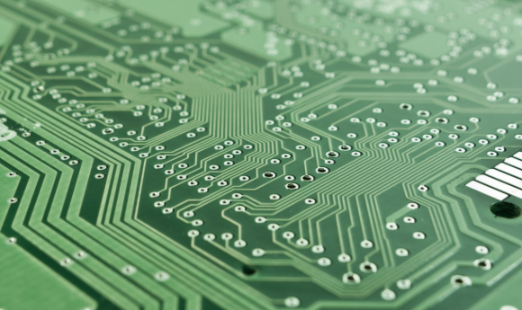
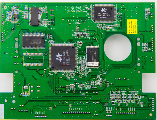
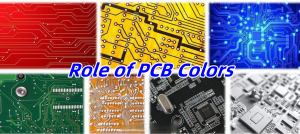
A common PCB board refers to the standard printed circuit boards widely used in various electronic devices. These boards are typically made from materials like FR4 (a flame-retardant epoxy laminate) and serve as the foundation for mounting and connecting electronic components. They are essential for creating functional circuits in everything from consumer electronics to industrial equipment.
What Are the Advantages of Common PCB Boards?
Common PCB boards offer several benefits, including:
- Cost-Effective: They are affordable to produce, making them ideal for mass production.
- Versatility: Suitable for a wide range of applications across industries.
- Reliability: Proven performance in various electronic devices.
- Ease of Design and Assembly: Simple to design and assemble, reducing production time.
- Durability: FR4 material provides excellent mechanical strength and resistance to heat and moisture.
Applications of Common PCB Boards
Common PCB boards are used in numerous industries, such as:
- Consumer Electronics: Smartphones, laptops, and home appliances.
- Industrial Equipment: Control systems, sensors, and automation devices.
- Automotive: Infotainment systems, engine control units, and lighting.
- Medical Devices: Diagnostic equipment and monitoring systems.
- Telecommunications: Routers, modems, and communication devices.

How to Make A Common PCB Board Prototype?
How to make a common PCB board prototype:
1. Design the Schematic & Layout
- Use free/low-cost tools like KiCad, EasyEDA, or DipTrace to draft the circuit schematic and PCB layout. Ensure component footprints match physical parts (e.g., SOIC-14 vs. DIP-14).
- Pro Tip: Include a 2–3mm border around the board edge for routing and mounting holes.
2.Generate Gerber Files
- Export industry-standard Gerber RS-274X and NC Drill files. Verify layers (copper, soldermask, silkscreen) using a free viewer (e.g., GerbView).
- Avoid: Hand-drawn sketches or non-standard formats (e.g., PDF) for fabrication.
3. Select Prototype-Friendly Materials
- Substrate: Choose FR-4 TG130–170 for cost efficiency. Avoid high-Tg or halogen-free materials unless required by design.
- Copper Weight: Use 1oz (35µm) for most prototypes—thicker copper adds unnecessary cost.
4. Choose a Fabrication Method
- Low-Cost Option: CNC routing for 1–5 pieces. Requires manual depanelizing but avoids tooling fees.
- Balanced Option: Chemical etching (ferric chloride or cupric chloride) for 5–20 boards. Use laser printer toner transfer for DIY projects.
- Avoid: Laser cutting for thick copper (>2oz) or tight tolerances (<0.2mm traces).
5. Order from a Prototype-Focused Shop
- Prioritize vendors offering 5–10 day turnaround with no MOQ. Confirm they accept 2–4 layer boards and standard finishes (HASL/ENIG).
- Red Flag: Suppliers charging setup fees for <50 pcs or refusing to review Gerbers pre-order.
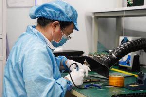
6. Assemble Components
- Manual Soldering: Use a hot air rework station for SMD parts (0402, QFN). Apply solder paste with a stencil or syringe.
- Automated Option: For >50 pcs, consider a local assembler with pick-and-place machines (costs $0.01–0.05 per pad).
7. Test & Debug
- Visual Inspection: Check for solder bridges, tombstoning, or lifted pads under a microscope.
- Functional Testing: Use a multimeter for continuity/shorts and a signal generator for high-frequency circuits.
- Fixes: Rework with desoldering braid or a desoldering gun. Avoid excessive heat (>300°C) to prevent pad lifting.
8. Document Iterations
- Label each prototype revision (e.g., “Rev A1,” “Rev A2”) and track changes (e.g., “Moved C1 closer to U1 to reduce noise”).
- Tool: Use GitHub or cloud storage to share Gerbers, BOMs, and test results with team members.
Why Choose Best Technology for Common PCB Boards?
As a leading common PCB board manufacturer, Best Technology is your trusted partner for high-quality common PCB boards. Here’s why:
- 18+ Years of Experience: With extensive expertise, we deliver reliable and innovative PCB solutions.
- Competitive Pricing: We offer top-quality products at the most affordable prices.
- No MOQ & Flexible Options: Whether you need prototypes or large-scale production, we accommodate all order sizes.
- 99% On-Time Delivery: We ensure your projects stay on schedule.
- ISO-Certified Quality: Our manufacturing processes adhere to ISO9001, ISO13485, and IATF16949 standards.
- Comprehensive Services: From design to assembly, we provide a one-stop solution for all your PCB needs.
- Customer-Centric Approach: Our goal is “Total Customer Satisfaction”, and we work closely with you to meet your requirements.

How to Reduce Production Cost of Common PCB Board?
Optimize Board Size & Shape
- Minimize dimensions: A 10% reduction in board area can lower material costs by 15–20%. Use DFM tools to auto-fit components within tighter boundaries.
- Avoid custom shapes: Rectangular or square boards waste less substrate than circular/hexagonal designs. Add mounting holes post-production if needed.
Standardize Component Placement
- Use common footprints: Prioritize SOIC, QFN, and 0805/0603 packages over BGA or QFP to reduce assembly complexity.
- Reduce layer count: Merge power/ground planes and reroute signals to eliminate unnecessary layers (e.g., 4-layer → 2-layer).
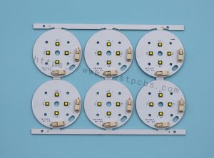
Leverage Panelization Efficiency
- Maximize panel utilization: Fill gaps with smaller boards or dummy coupons. A 500x600mm panel can fit 40% more 50x50mm boards with optimized nesting.
- Adopt V-scoring: Reduce depanelizing labor costs by 80% compared to routing.
Negotiate Material Costs
- Bulk purchase FR-4: Commit to 3–6 month supply agreements for 5–10% discounts.
- Recycle scrap: Partner with local recyclers to sell copper-clad waste (typically $1–2/kg).
Automate Production Steps
- Invest in SMT lines: A 50K–100K pick-and-place machine reduces assembly labor by 70% for >1K units/month.
- Use AOI systems: Automated optical inspection cuts quality control costs by 50% vs. manual checks.
Simplify Surface Finishes
- Choose HASL over ENIG: Saves 0.05–0.10 per board. Avoid gold for non-critical contacts.
- Omit peelable mask: Use taped stencils instead for selective soldering.
Outsource Non-Core Processes
- Partner for plating: Send boards to specialists for ENIG/immersion tin if in-house setup costs exceed $20K.
- Use contract manufacturers: For <500 pcs/month, CM fees (15–25% of BOM cost) may offset internal labor/equipment expenses.
Reduce Testing Complexity
- Limit flying probe tests: Use bed-of-nails fixtures for high-volume runs (costs 500–1K but reduces per-unit testing time by 60%).
- Skip impedance testing: Unless designing for high-speed signals (e.g., USB 3.0, HDMI).
Implement Lean Inventory
- Adopt JIT (Just-in-Time): Align component orders with production schedules to avoid holding costs (typically 20–30% of inventory value).
- Use kanban systems: Reorder materials when stock reaches 10–15% of buffer levels.
Our Services
At Best Technology, we offer a full range of services for common PCB boards, including:
- PCB Design: Customized designs tailored to your specifications.
- PCB Prototyping: Fast and accurate prototyping to test your designs.
- PCB Manufacturing: High-quality production with advanced technology.
- PCB Assembly: Complete assembly services for seamless integration.
- Component Sourcing: Reliable sourcing of high-quality components.
- Testing and Inspection: Rigorous testing to ensure performance and reliability.
Contact Us Today
For high quality common PCB boards, trust Best Technology as your reliable partner. Contact us today to discuss your project requirements and get a quote: sales@bestpcbs.com.
You may also like


Tags: Common PCB Board