If you’ve ever tried to get a copper core PCB prototyped, you might have experienced sticker shock. Compared to standard FR4 or even aluminum PCBs, copper base PCB prototyping is significantly more expensive. But why is that? Is it just the material cost—or is there more behind the pricing?
This article explores why copper core PCB prototyping is expensive, highlighting the five core factors that affect the price. If you’re planning to prototype with copper, this guide will help you manage expectations and control costs without compromising quality.
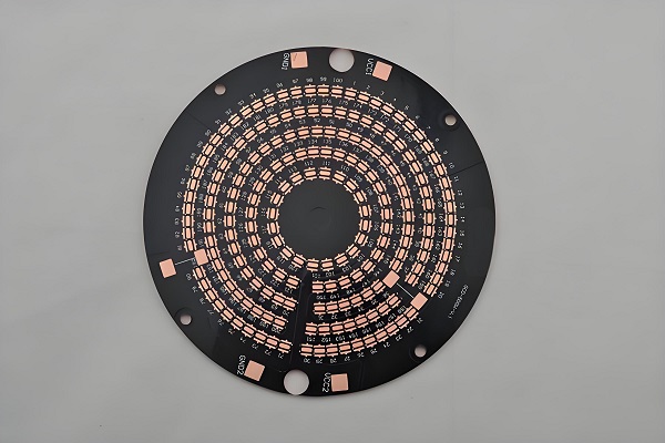
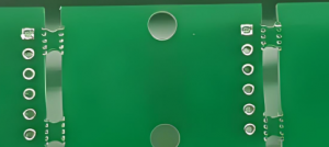
1. High Raw Material Cost of Copper Base PCB
Copper is a premium metal. Compared to aluminum or traditional FR4 materials, copper base PCBs use significantly more raw copper, especially for heavy copper designs (2oz to 10oz). Thick copper requires more material, which increases raw material cost.
Besides the copper layer, these PCBs often use advanced insulation materials like ceramic or high-conductivity epoxy, which are not cheap. Together, they make copper base PCB a costlier substrate right from the start.
2. Copper Core Is Costlier and Harder to Process
Copper base PCBs are built on metal substrates where copper is used as the base material. Compared to aluminum PCBs, copper-based substrates have higher thermal conductivity and mechanical strength—but also come at a premium.
Challenges:
- Copper is heavier and more difficult to machine than aluminum.
- It demands higher-grade dielectrics to manage heat flow and electrical insulation.
- Machining tolerance must be tight, which often requires CNC milling or laser cutting.
In prototyping, every material switch requires reprogramming and tool setup—this adds to unit cost, especially for small batches.
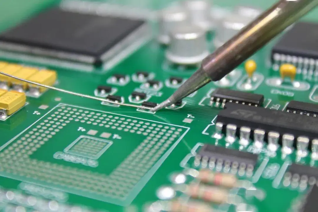
3. Full-Process Manufacturing for Low Volumes = High Unit Cost
Many customers expect prototyping to be a simplified process, but copper PCB prototypes go through the full manufacturing workflow, just like mass production.
Involved Steps:
- Lamination of copper foil and dielectric layer onto the metal core
- Photolithography and etching of thick copper traces
- Drilling and metal plating through holes (if applicable)
- Solder mask and silkscreen application
- Surface finish such as HASL, ENIG, or OSP
- Electrical and AOI testing
Unlike FR4 samples, these steps for copper PCBs are more labor-intensive and require custom setup, making short runs costly.
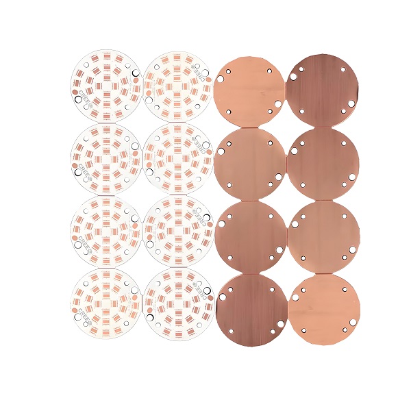
4. Board Size and Quantity: Small Orders Still Use Full Panels
You might think that fewer boards mean lower cost—but that’s not how copper PCB prototyping works. Manufacturers need to process entire panels, even if the customer only needs one or two pieces.
Key Considerations:
- Panel utilization is poor for unique shapes or non-standard sizes.
- Tooling, drilling, and routing costs remain fixed regardless of quantity.
- Wasted copper material adds to the final quote.
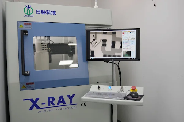
5. Testing and Quality Control Requirements Raise the Bar
Copper base PCBs are commonly used in high-power LED lighting, automotive control units, power supplies, and military devices. These applications demand precise thermal performance, which must be verified in prototypes.
Extra Testing:
- Dielectric strength and thermal conductivity evaluation
- X-ray or AOI inspections to verify copper-to-core bonding
- Flatness and planarity checks
- Anti-oxidation packaging for copper exposure protection
While FR4 or aluminum PCBs may pass with visual inspection, copper PCB prototyping requires intensive quality checks to simulate performance under real-world stress.
In addition to this, only a small percentage of PCB manufacturers have the equipment, technology, and skilled workers to prototype copper base PCBs. These facilities often run specialized machinery and require higher operational overheads. That exclusivity creates a supply-demand gap, increasing pricing. Furthermore, setup for copper PCBs takes more time — involving tool calibration, stack-up configuration, and thermal modeling — all of which raise prototyping expenses.
How to Lower Your Copper PCB Prototyping Cost?
While you can’t eliminate the inherent cost of copper core PCB prototyping, you can definitely make smart choices to reduce waste and improve cost-efficiency. Here are strategic steps engineers and procurement teams can take:
1. Choose the Right Copper Thickness
Avoid overengineering. While 5oz or more copper might seem safer, most designs perform well with 2oz to 3oz copper thickness. This keeps etching time, material use, and plating costs within reason.
2. Standardize Your Board Shape and Size
Odd-shaped PCBs or extremely small panels lead to poor panel utilization. Try to stick to standard sizes like 100mm x 100mm or 150mm x 150mm, which optimize production yields and reduce cutting loss.
3. Simplify the Initial Design
Avoid complex features such as plated through-holes, cavities, or selective surface finishes in your prototype stage. These features add cost and are often not required for first-round validation.
4. Use Cost-Efficient Dielectrics
For less heat-sensitive applications, consider standard ceramic or polymer-based insulation layers rather than high-cost options like AlN unless required. Choosing the right dielectric saves material and processing time.
5. Avoid Over-Specifying Surface Finishes
Electroless Nickel Immersion Gold (ENIG) is often used, but it’s not always necessary. If you don’t need high wire bonding or long shelf life, consider OSP or HASL—these finishes are far more affordable.
6. Batch Your Orders to Improve Panel Utilization
If you plan to order multiple revisions or versions, ask your manufacturer if they can combine them in a single panel. This reduces setup time and improves manufacturing efficiency.
Why Choose Best Technology for Copper Core PCB Prototyping?
At Best Technology, we specialize in copper base PCB manufacturing and prototyping. We understand the thermal, electrical, and mechanical demands of your application—and we’re here to support you at every step.
Our Advantages:
- In-house CNC machining for precise panel shaping
- Extensive material inventory including standard and heavy copper
- MES traceability and full-process quality inspection
- Thermal simulation support before prototyping
- Global shipping with vacuum-sealed packaging
- One-on-one engineering consultation for design reviews
- Free DFM & DFA checks
We’re certified under ISO9001, ISO13485, IATF16949, and AS9100D, making us a reliable partner for medical, automotive, and aerospace industries.
Conclusion
If you’re planning to develop high-power or heat-sensitive electronics, copper core PCB prototyping is a strategic investment. While the costs may seem high initially, understanding the five main cost factors gives you more control over your design and procurement decisions.
Looking to reduce the copper PCB sample price while maintaining performance? Contact Best Technology for a free quote and technical design review.
Frequently Asked Questions (FAQs)
1. Why is copper base PCB prototyping more expensive than aluminum PCB samples?
Copper is costlier and harder to machine. It also needs special insulation materials and more precise control during manufacturing, which adds to the overall expense.
2. Can I use thinner copper to reduce prototyping costs?
Yes, 2oz or 3oz copper works well for most thermal and current needs. Always confirm with your PCB supplier.
3. Is SMD-only design more cost-effective for copper PCBs?
Absolutely. Using SMD components eliminates through-holes and makes the manufacturing process simpler and cheaper.
4. How can I estimate copper PCB prototyping cost?
Submit your Gerber files, copper weight, board dimensions, and finish requirements to your supplier for an accurate quote.
5. What files should I provide to the manufacturer?
You should prepare and send your Gerber files (RS-274X), drill file, copper thickness, stack-up details, fabrication notes, and BOM (if assembly is needed). This ensures fast and accurate quotation and fabrication.