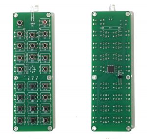
The test point is designed to test the components of the PCB if they meet the specifications and solder mask or not. For example, if we want to check a resistance on the circuit board if have any problem, the easiest way which is use the universal meter to measure the both ends of PCB. But if there have a large number of PCBs, it is hard to use the universal meter to test each components are correct or not one by one. So we can use the automated test machine of ICT(In-Circuit-Test) to test, which is designed by probe (normally called “needle Bed (Bed – Of – Nails)” fixture). This test machine can test all the circuit of components on the PCB at the same time. Then through the way of program control to measure the characteristics of the components. Generally speaking, the PCB only need to take around 1-2 minutes to finishih the testing. The testing time are depending on the components’quantity, the time will be more longer with the more components.
But if the probe contact with the components or solder pads on the PCB directly, it will damage some components easily. So the engineers design the “test point†on the PCBs, which is designed the additional parts to elicit a pair of round on the both ends of components, and there is no solder mask. It can contact these small test points directly and measure the components by the probe.