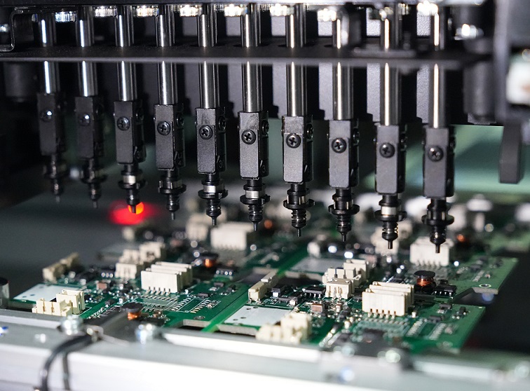
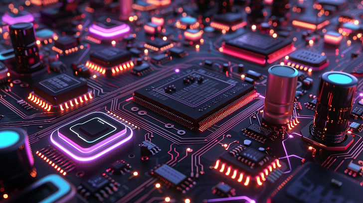
A motherboard network adapter PCB comprises several key components, each playing a vital role in ensuring effective network connectivity. And between them, the PCB is the most important. Now, best technology is sharing an example about motherboard network PCB design.
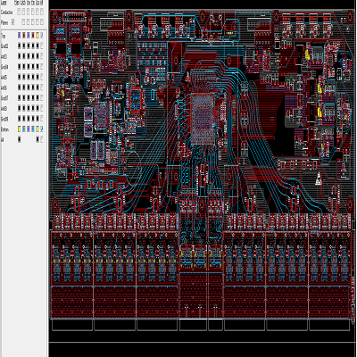
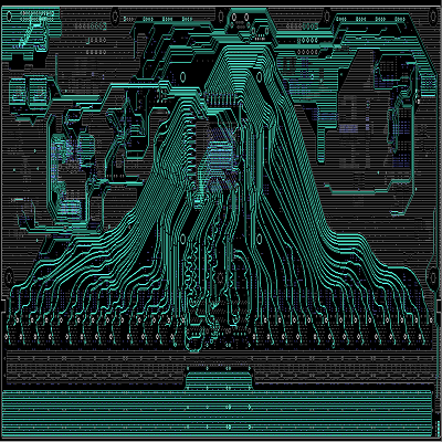
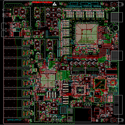
10G/100G large capacity convergence shunt
[1]: Marvell: 98DX8548
[2]: 21A maximum current
[3]: Single pair differential line, 10G and 25G optical networks
[4]: 10 layers PCB
What are the considerations before PCB design?
PCB design involves several steps and some considerations need to be noticed. If you are a designer, think about these points before starting the design.
Manufacturing: prototyping study or mass production.
What it will be used in?
What kind of production technology it will used?
Material?
How many layers you want?
Whether need to do impedance control?
EBest Circuit (Best Technology) has more than 17 years in this industry, we have served for over 1200 customer all around the world. Our goal is to provide customer with best solutions and top notch quality products, and it is luckily that we did a good job. If you want to work with us or need a PCB manufacturer in Asia, contact us right now!
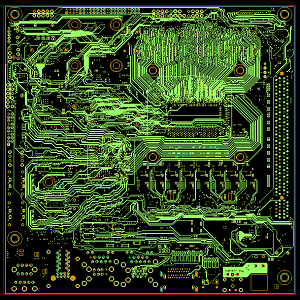
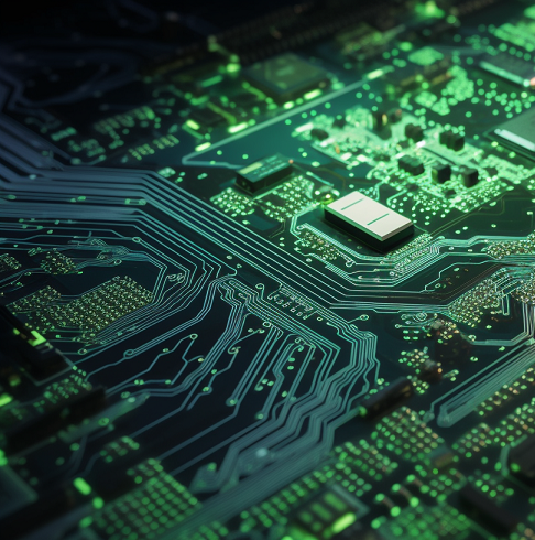
A high-speed circuit handles signals that switch quickly or operate at high frequencies, typically above 50 MHz, though some advanced systems may go into the GHz range. EBest Circuit (Best Technology) is a one-stop PCB manufacturer that covers pcb design, pcb layout, pcb diagram, DFM, SI, PI analysis, PCB manufacturing and so on. In the following, you can see a high speed pcb design solution for industrial switch that we cooperated with our customer.
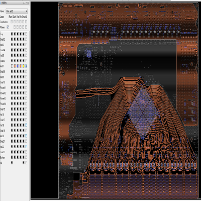
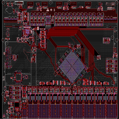
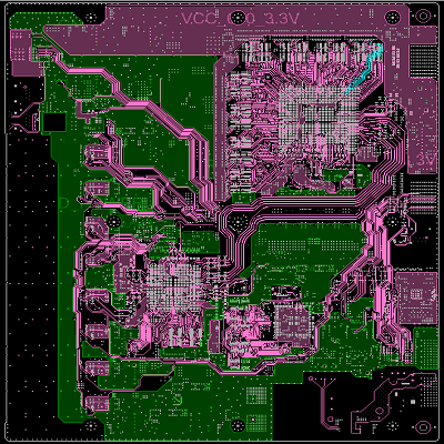
32 x 400GE industrial switch
[1]: Marvell-400G chip
[2]: 200A maximum current
[3]: Single pair differential line 56G optical network
[4]: 24 layers high power PCB
What’s the Best Material for High-Speed PCB Design?
Choosing the right material is vital for maintaining signal integrity and achieving optimal performance. The material impacts the board’s dielectric constant (Dk), loss tangent, and overall signal quality. Common materials include:
FR4: Widely used but not ideal for very high frequencies due to higher loss tangent.
Rogers (RO4000 series): Preferred for high-speed designs thanks to its low dielectric constant and loss tangent.
Teflon: Excellent for high-frequency applications but more expensive and harder to process.
Selecting the appropriate material ensures the PCB can handle high-speed signals without compromising performance.
For the PCB design service, we can make sure the one-time success to save much time and money for customers. Our goal is to work with customers together and win more market with our clients. Just feel free to contact our technical team if you have similiar designs.
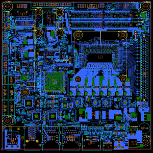
Best technology offers numerous PCB design solutions for our customer, from HDI design, high speed device PCB design, AI optical module design and network motherboard design for network switching. Below is one of our network motherboard design solutions:
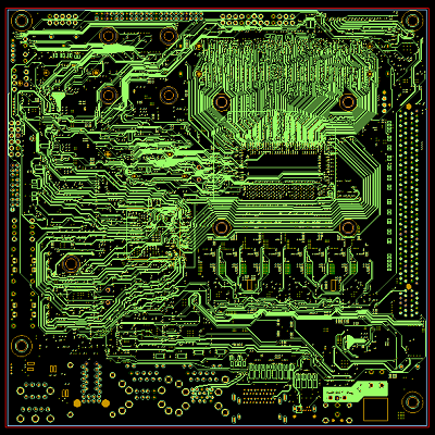
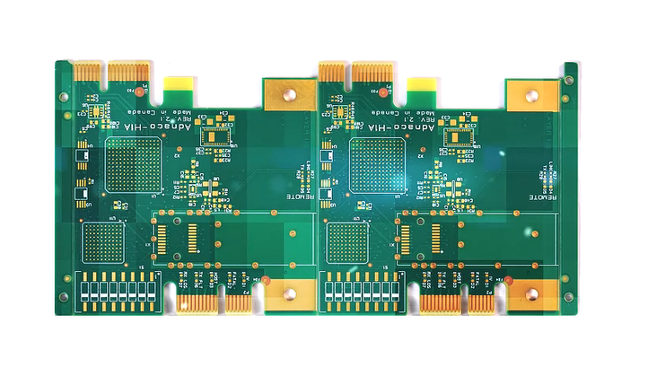
An ATCA network switching motherboard
[1]:BCM88XXX, BCM55XXX chips
[2]:60A maximum current
[3]:8口10G optical network
[4]: 8 x DDR3 chips
Network Switching Differential Pair Design Guide
Each TrxP/TrxN signal group (where xcx0-3) shall be routed as a differential pair. This includes the entire length of wiring processing.
The individual differential correspondences are packed together as tightly as possible. Impedance calculations are usually started by selecting the smallest line blank (4-5mil). The tracking width is then adjusted to achieve the necessary impedance.
Differential line group resistance of Ethernet is calculated at 100 ohms.
In general, when routing the four differential pairs of the Gigabit Ethernet to the r45 connector, at least one pair will pass through to the opposite outer layer.
Priority should be given to differential pair wiring. Terminals should be added after the routing is determined
The values of all resistance terminals in the Ethernet front end should be 1.0% tolerance
All capacitor termination Ethernet front ends in the module should have strict tolerances and high quality product media (npo)
You are welcome to contact us if you want to get your DIY network switching PCB designs.
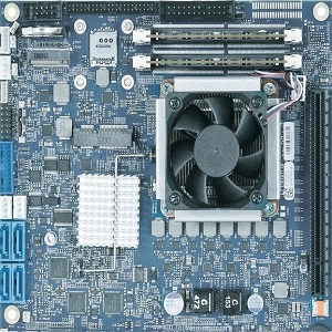
Best technology engaging in the PCB manufacturing and PCB design for more than 17 years. With a strong R&D team, we can provide customers with fast and valued PCB design solutions. Here is one of our industrial motherboard design & industrial PCB case sharing for your reference. If you want to get your own industrial PCB design, welcome to contact us.
A mITX architecture industrial control motherboard
[5]:2x USB 3.0 (Internal) + 1x USB 3.0 (Client) + 2x USB 3.0 (Rear I/O) + 2x USB 2.0 (Rear I/O) +
2x USB 2.0 (Front Header) + 1x USB 2.0 (mPCIe)
Industrial PCB Design Considerations
Control the length of the circuit: Minimize the length of the circuit, especially the key signal lines, to reduce signal attenuation and delay.
Avoid sharp angles and right angles: Right angles and sharp angles should be avoided when wiring, and rounded or 45 degree angles should be used as far as possible to reduce signal reflection and impedance discontinuity.
Line width: Determine the line width according to the current size and thermal requirements to ensure the reliability and stability of the circuit.
Inter-layer wiring: Rational use of multi-layer PCB inter-layer wiring, such as the signal line on the inner layer, power and ground wire on the outer layer.
Impedance control: For high-speed signals, it is necessary to control the line impedance to ensure signal integrity, and carry out impedance matching design if necessary.
Avoid cross and parallel wiring: Try to avoid cross and parallel wiring of signal lines to reduce crosstalk and electromagnetic interference.
Contact us if you have any questions and inquiry about industrial PCB design projects.
PCB design not only including the routing layout, component placement also is a key parameter. It involves understanding electrical parameters, signal integrity, and thermal management. This article will introduce several golden rules of how to optimize your component placement, whether you are a novice or a seasoned professional, it is helpful for you to manage your circuit board design greatly.
Determine the power supply and grounding plane
In the early stage of PCB design, reasonable power supply and grounding layout is the key. The power supply and ground plane not only provide a stable power supply for the components, but also play a role in reducing electromagnetic interference (EMI). To begin the layout, the first thing is confirming the location of the power supply and ground area. Usually, the power is placed in a complete layer of the PCB, and the ground is in another layer, which can effectively reduce the power supply noise.
Make sure the power plane is close to the area where high power is needed, which can reduce the voltage drops along the supply path. The ground area should be as large and continuous as possible, this helps to provide a good return path and reduce interference from high-frequency signals.
Differentiate layouts by function
When laying out components, dividing the circuit board into different functional areas can improve the efficiency and performance of the design. For example, you can separate power supply into signal processing area, power management area, and interface. This method helps to reduce the mutual interference between different circuits and improve the overall stability of the circuit.
Please noted that, high-frequency components should be close to connectors or key interfaces to shorten the signal path and reduce interference. Low-frequency components can be placed away from critical signal paths to optimize overall signal integrity.
Keep short and direct trace
Shortening the length of signal lines is another important thing to optimize component layout. Make sure keep them short and direct as possible. Long distance signal routing may lead to signal attenuation and delay, which will affect the overall performance of the circuit. Placing the relevant components as close as possible. This not only reduces the length of the circuits, but also reduces the coupling and interference between the signals.
In addition, in the routing process, try to avoid right-angle (90 degrees) turns. Because the right angle will cause signal reflection, affecting the integrity of the signal. Try to use 45 degree turns or arc turns to reduce signal loss.
Consider heat dissipation requirements
Heat management is an important consideration when placing high-power components. Place power components in the edge area of the PCB, such as power transistors and high-frequency converters. This facilitates the use of natural air flow for heat dissipation and convenient for the installation of external cooling devices.
In high-density designs, through-holes, vias and cooling copper blocks can be designed on the PCB, which can transfer heat to the inner layer or bottom of the PCB to help dissipate heat. In addition, maintain a reasonable distance between each component to promote air flow and heat dissipation.
Optimize test points position
Consider placing test points in a convenient location for testing and debugging. Placing test points close to relevant components simplifies the debugging process and reduces test complexity. In particular, the placement of test points on the key signal path can facilitate the detection and verification of signal integrity and stability in the design stage.
For example, the discrete components required for OpAmp operational amplifiers can be placed close to the device, so that the bypass capacitors and resistors can work with them. This helps to optimize the wiring length mentioned as above, while also making testing and fault detection easier.
Consider DFM & DFA factors
Optimizing component layout takes into account not only electrical performance, but also the actual requirements of manufacturing and assembly. For example, try to avoid placing components on both sides of the PCB to simplify the PCBA assembly process. The components are arranged neatly and spaced consistently, which helps the automated assembly equipment to operate efficiently and reduce assembly errors.
Properly using DFM (Design for Manufacturability) principles make production easier and more cost-effective. Ensure that your design can be fabricated with standard processes.
Perform DRC as often as possible
Although it only takes a short time to run DRC (Design Rule Check) functionality on PCB software. But in some complex design environments, perform checks during the design process can save a lot of time, which is a good habit to keep. Every layout routing decision is critical, and running DRC can remind you of the most important layout at any time.
Check production files before sending to manufacturer
While most of PCB manufacturers are happy to download it directly and verify it for you, it is best to export the Gerber file yourself and use the free software such as Gerberv to check that it is as expected to avoid misunderstandings. By verifying it yourself, you may even find some inadvertent errors and thus avoid the cost of completing the production according to the wrong parameters.
[5]:2x USB 3.0 (Internal) + 1x USB 3.0 (Client) + 2x USB 3.0 (Rear I/O) + 2x USB 2.0 (Rear I/O) +
2x USB 2.0 (Front Header) + 1x USB 2.0 (mPCIe)
Anyway, communicating with your manufacturer to understand their equipment and processes can optimize the design, reduce manufacturing problems, improve production efficiency and product quality.
Although semiconductor integration is increasing, many applications have ready-to-use systems on chip. And there are various powerful and out-of-the-box development boards are becoming more readily available, many use cases in electronics still require the use of custom PCBs. In one-time development, even an ordinary PCB can play a very important role. This article will introduce several golden rules of PCB design, and are widely applicable to various PCB design projects.
What are the golden rules of PCB design?
The golden rules of PCB design serve as the foundation for a robust layout. Remember below top 5 rules can help you in PCB designing.
Optimize component placement
Select correct crosstalk
Make sure short and straight circuits
Manage the distribution of power and ground circuit whenever possible.
Avoid sharp angles in traces, opting for 45-degree turns instead.
Additionally, always perform Design Rule Checks (DRC) to catch potential issues before finalizing the layout. These checks help ensure compliance with manufacturing and performance standards.
What are the top 3 important steps in PCB design and layout process?
The PCB design and layout process has many important steps, but these three processes should be given priority.
1. Schematic design and component selection
Start by creating a detailed schematic diagram of your circuit board. As a designer, you can choose discrete components with high or low component values, but with the same performance. By consolidating within a smaller range of standard values, the bill of materials (BOM) can be simplified and potentially cost reduced.
Select suitable components based on the requirements of your design, considering factors like voltage, current, and signal frequency. A clear and precise schematic is essential. It helps avoid errors and streamlines the layout process, making it easier to place and route components effectively.
2. Component placement
Arrange components strategically on the board. Place critical components like microcontrollers and high-frequency ICs first, followed by supporting components. Consider heat dissipation and accessibility for debugging. If you have a range of PCB products based on preferred component values, it will also help you make the right inventory management decisions in the longer term.
3. Routing
Routing including connecting the components with traces. Prioritize routing for critical signals first, such as clock lines and high-speed data paths. Use the shortest possible paths and avoid crossing different signal types to reduce interference. After critical traces, route the power and ground nets, followed by less critical signals. Utilize multiple layers if needed to keep the layout clean and manageable.
What are the guidelines for PCB layout?
PCB layout guidelines can help designers achieve optimal component placement and ensure the board is easy to assemble. Here are some things to consider:
1. Trace width and spacing
Maintain appropriate trace width and spacing based on current carrying capacity and voltage levels. The IPC-2221A standard provides recommendations on PCB trace width and spacing. According to this standard, the trace width must be selected based on current-carrying capacity and permissible temperature rise. For instance, a 1mm wide trace with 1oz. copper (35μm) can carry approximately 2.5A with a 10°C temperature rise.
2. Layer stack-up
Design your PCB stack-up carefully. Multilayer designs are typically used in high-frequency applications to effectively separate power, ground, and signal layers, thereby reducing electromagnetic interference (EMI). Studies show that in a 4-layer or more stack-up, closely coupling the power and ground planes can significantly reduce EMI and improve signal integrity.
3. Thermal management
Consider thermal aspects in your layout. Place components that generate significant heat, such as power transistors, away from heat-sensitive components. Use thermal vias and heat sinks to manage heat dissipation effectively.
4. Via placement
Use vias strategically to connect different layers. Avoid placing too many vias close to high-frequency signal paths to prevent signal degradation. Use via stitching to enhance ground planes and reduce loop areas.
5. Power distribution
Using wide traces for power and ground planes is critical to minimizing resistance and inductance. For instance, IPC-2152 provides guidelines on power distribution and suggests using wide traces to handle higher currents and minimize voltage drops.
What are the considerations of PCB layout?
When designing a printed circuit board, you can consider these points:
1. Signal integrity
Maintain signal integrity by minimizing trace lengths and avoiding impedance mismatches. Use differential pairs for high-speed signals and keep them close together to reduce noise.
2. EMI/EMC
EMI and EMC are critical considerations. Use proper shielding and grounding techniques to mitigate interference and ensure compliance with regulatory standards.
3. Design for Manufacturability (DFM)
Ensure your layout is manufacturable by adhering to fabrication capabilities and tolerances. Simplify routing and avoid excessive component density to facilitate easier assembly and inspection.
4. Mechanical constraints
Consider the physical dimensions and mounting requirements of your PCB. Ensure that components and traces do not interfere with mechanical parts or enclosures.
5. Cost
Optimize your design for cost by reducing layer count where possible and minimizing the use of expensive materials or processes. Balance performance requirements with budget constraints.
At EBest Circuit (Best Technology), we offer expert design services to help you achieve your project goals with precision and excellence. Choose us for your next PCB project and experience the benefits of quality and innovation.
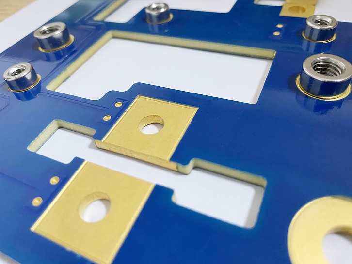
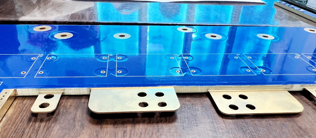
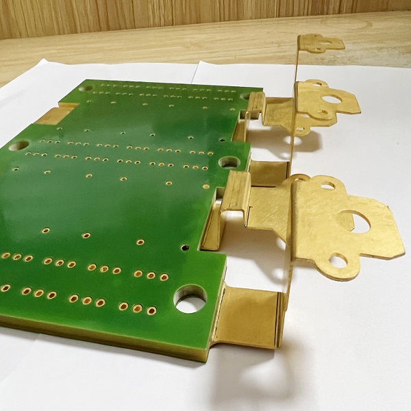
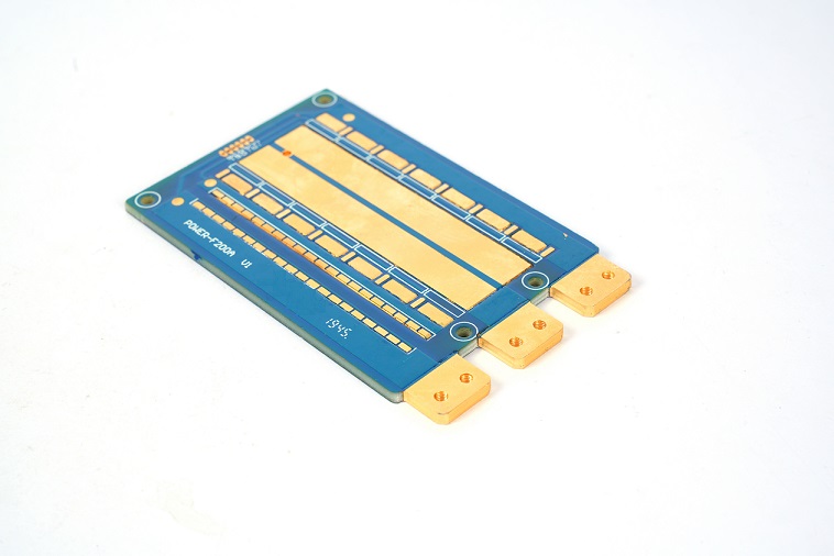
In the electronics industry especially for new-energy vehicles, a Bus Bar PCB plays an important role to achieve specific function. It transmits large amounts of current through metal strips or conductive paths, making it ideal for high-power applications. The design of busbar PCBs is a key technical area for designers or engineers who engaged in power distribution or who require efficient current management. In this article, we would like to share some information about the considerations during a bus bar circuit board designing, hope this may help you to design a desired PCB successfully.
What is a Bus Bar PCB?
Bus bar PCB is one of a new type of heavy copper PCB and it was made by FR4 fiber glass material and laminated with metal alloys. It transmits electrical energy from one point to multiple output points through integrated conductive paths, which are typically made of copper or aluminum. Busbar PCBs are designed to reduce resistance and inductance, thereby maximizing current transfer efficiency and minimizing energy loss.
Generally, if it is used in a charging pile product, there are generally at least 2 busbar circuit boards, one is the main control board (a larger one), and the other is a smaller board, both of two need to use the bus bar process.
Bus bar PCB is widely used in power distribution systems, electric vehicles, industrial equipment and other occasions requiring high current. They are designed to simplify system wiring, reduce electromagnetic interference (EMI), and improve overall reliability and performance of the product.
Why is High Current Bus Bar PCB Important?
Bus bar PCB has irreplaceable advantages in current transmission and power distribution. They mainly feature three functions when used in electronics. First of all, they are able to efficiently handle large currents without generating excessive heat. This is what standard FR4 PCB cannot achieved. Secondly, bus bar PCB has ability to significantly reduce the complexity of the circuit layout design. By integrating the current transfer path, they can reduce the number and length of circuits required by the system, thereby simplifying system design and reducing potential failures.
In addition, bus bar PCB helps reduce electromagnetic interference. Due to the design optimization of the conductive path, the noise generated during current transmission can be effectively suppressed. This characteristic makes it perform well in high-noise environments, ensuring the stability and reliability of electronic devices.
What Should We Consider When Designing A Bus Bar PCB?
Due to it is a new innovation in the industry, it is a not a simple thing to design a bus bar circuit board successfully. It’s a complex task that requires consideration of several technical factors to ensure its effectiveness and reliability. The following are the main aspects to focus on when designing a bus bar PCB.
Copper Thickness
The first important thing is what’s the copper thickness of busbar you want to. You must know, thicker copper allows for higher current carrying capacity, but not thicker thickness is better, it should be calculated according to the voltage and current it will used in.
Current capacity and temperature management
The bus bar PCB should be designed to carry the maximum expected current while keeping the temperature within a safe range. This is usually achieved by selecting the appropriate conductor material and optimizing the cross-sectional area of the conductor. For example, for 100A current requirements, a typical design would use copper strips with a thickness of 5mm to ensure that the temperature rise does not exceed 20C.
Resistance and inductance
Low resistance and low inductance are key to bus bar PCB design. The shape, thickness and layout of conductors should reduce resistance and inductance as much as possible to improve the efficiency of current transmission. For example, the use of trapezoidal or flat conductors can effectively reduce inductance, thereby improving current transmission performance.
Electromagnetic compatibility (EMC)
Bus bar PCB design also needs to consider electromagnetic compatibility issues to ensure that it does not produce too much electromagnetic interference (EMI), while being able to resist external electromagnetic interference. By optimizing the conductor layout and using shielding materials, the electromagnetic compatibility of the bus PCB can be significantly improved.
Thermal management
Because bus bar PCB aims to transmit high current, thermal management is an important part of the design. The thermal design should ensure that the PCB can effectively dissipate heat and prevent overheating damage. For high power applications, radiators or active cooling are often used to ensure temperature control within design specifications.
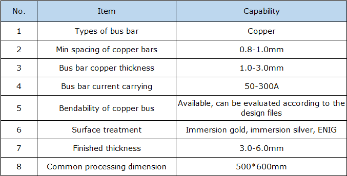
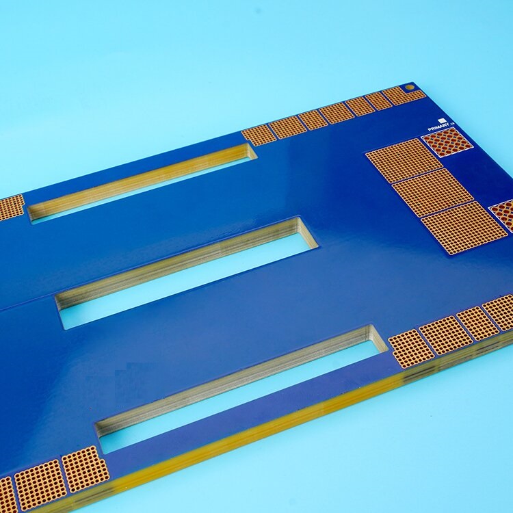
EBest Circuit (Best Technology) Manufacturing Capability of Bus Bar PCBs
As the one of leading PCB manufacturers in China, EBest Circuit (Best Technology) has exceptional capabilities in the production of busbar PCBs. Our manufacturing capabilities include high-precision metal processing technology to produce busbar PCBs with complex geometry and tight tolerances. In addition, we also have the production capacity of multi-layer bus bar PCB to meet the needs of different applications.
EBest Circuit (Best Technology) is committed to providing customers with high-quality, high-performance busbar PCBs to support their power management and distribution systems. Below is a basic parameter of our bus bar PCB manufacturing capability. For more details, welcome to e-mail us at sales@bestpcbs.com.
(Best technology capability of bus bar pcb)
Nowadays, bus bar PCBs are widely used in power distribution systems, electric vehicles, industrial equipment and other occasions requiring high current. According to statistics, the global busbar market is expected to grow at a compound annual growth rate (CAGR) of 6.5% between 2023 and 2028, demonstrating the growing importance of this technology in multiple industries.
With the rapid development of the eras, the most important thing for designers or buyers is to find a reliable bus bar PCB manufacturer to meet the high demands of the market. As the expert of the bus bar PCB fabricating, EBest Circuit (Best Technology) has the mature technology and advanced equipment to produce high quality bus bar PCBs. Contact us right now to get your own bus bar PCB solutions!
High-Density Interconnect (HDI) PCBs are revolutionizing the electronics industry with their advanced capabilities and compact designs. As technology continues to evolve, the demand for smaller, faster, and more efficient electronic devices has led to the widespread adoption of HDI PCBs.
What is Definition of HDI PCB?
HDI board refers to High Density Interconnect, that is, high density interconnect board, which is a relatively new technology developed by the PCB industry at the end of the 20th century.
The drilling of the traditional PCB board is affected by the drilling tool, and when the drilling aperture reaches 0.15mm, the cost is already very high, and it is difficult to improve again. The drilling of HDI board no longer relies on traditional mechanical drilling, but uses laser drilling technology. (This is why it is sometimes called a laser plate.) The hole diameter of the HDI board is generally 3-5mil (0.076-0.127mm), the line width is generally 3-4mil(0.076-0.10mm), the size of the pad can be greatly reduced, so more line distribution can be obtained within the unit area, and the high-density interconnection comes from this.
Smaller device spacing, more I/O pins and embedded passive devices Larger ASiCs and FPGAs with increasingly shorter rise times and higher frequencies all require smaller PCB feature sizes, which is driving a strong demand for HDI/ micro through-holes. The typical high density interconnector designs are including:
1+N+1
2+N+2
3+N+3
4+N+4
What are the benefits of HDI PCB?
HDI is a compact circuit board designed for small volume users. Compared with ordinary FR4 PCB, the most significant feature of HDI is the high wiring density, and the difference between the two is mainly reflected in the following three aspects.
1. HDI is smaller and lighter
HDI board is a traditional dual panel as the core board, through continuous stacking layer by layer. This kind of circuit board made by continuous layering is also called Build-up Multilayer (BUM). Compared with traditional circuit boards, HDI circuit boards have the advantages of “light, thin, short and small”.
The electrical interconnection between the HDI board is realized through the conductive through hole, buried hole and blind hole connection, its structure is different from the common multi-layer circuit board, and a large number of micro-buried blind holes are used in HDI board. HDI uses direct laser drilling, while standard PCBS usually use mechanical drilling, so the number of layers and aspect ratio tend to be reduced.
The high density of HDI board is mainly reflected in the hole, line, pad density, and layer thickness.
● Micro-via hole
The HDI board contains the design of micro-pilot holes such as blind holes, which is mainly reflected in the micro-hole formation technology with a diameter less than 150um, and the high requirements of cost, production efficiency and hole position precision control. In the traditional multilayer circuit board, there are only through holes and no tiny buried blind holes.
● Fine line width and line distance
Its main performance in the wire defects and wire surface roughness requirements are more and more stringent. Generally, the line width and line distance do not exceed 76.2um.
● High pad density
The density of welded contacts is greater than 50 per square centimeter.
● Thinning of medium thickness
It is mainly manifested in the trend of the thickness of the interlayer medium to 80um and below, and the thickness uniformity requirements are becoming more and more stringent, especially for high-density plates and packaging substrates with characteristic impedance control.
2. Better electrical performance
HDI not only enables end-product designs to be miniaturized, but also to meet higher standards of electronic performance and efficiency at the same time.
The increased interconnect density of HDI allows for increased signal strength and improved reliability. In addition, the HDI board has better improvement for RF interference, electromagnetic wave interference, electrostatic discharge, heat conduction and so on. HDI also uses full digital signal process control (DSP) technology and a number of patented technologies, with a full range of load adaptability and strong short-term overload capability.
3. The HDI board has very high requirements for buried holes
It can be seen from the above that whether it is the volume of the board, or the electrical performance, HDI is better than ordinary PCB. Where the coin has two sides, the other side of HDI is as a high-end PCB manufacturing, its manufacturing threshold and process difficulty are much higher than ordinary PCB, and there are more problems to pay attention to when producing – especially the buried hole jack.
What are the basic parameters of HDI PCB?
HDI PCB has greater different with normal FR4 PCB, from the stack up, material selection, manufacturing and cost. So, it is vital to understanding the basic parameters of a high-density interconnect board before start your designing trip. The standard parameters of HDI board mainly include the following aspects:
Numbers of layers
Generally, the number of layers of HDI board is 4-20 layers, and the high-end HDI board can reach to 40-50 layers.
Line width/spacing
Due to the HDI PCB are always used in high-end applications, their line width and spacing are usually very strict, and the common requirement is that the line width/spacing is 4/4mil (0.1mm), or even smaller.
Blind hole, buried hole, bus
These are one of the characteristics of the HDI board, blind hole and buried hole can reduce the area of the circuit board, make your design more density, and the bus enable to improve the signal transmission rate of the PCB.
Board thickness
The board thickness of HDI board is usually range from 0.8 to 3.2mm, of which 1.6mm is the most common thickness.
Pad
The pad on the HDI board is generally very small, and the common pad size is 0.2mm to 0.5mm. Different factory has different capabilities, it is best to ask your supplier or manufacturer to get a manufacturing capability document.
Impedance control
For high-speed signal transmission circuits, the impedance control of the HDI board is very important, and the requirements are very strict. It is needed to tell your vendor if your HDI board will be used in high-speed devices.
Material
The main materials of HDI board are FR4, BT, PI, PET, etc. Different materials can meet different requirements.
This is the end of this sharing, contact us today to learn more about our HDI PCB solutions and how we can help you achieve your technological goals. In our next chapter, we will introduce the manufacturing process and methods of HDI boards, let me know if you are interested in it.
With the continuous growth of new energy demand and the transformation of energy structure, the market size of high-power technology continues to expand. The high power pcb includes heavy copper pcb, bus bar pcb. As an important part of the battery module in the energy storage system, the high power PCB plays a key role in the safety and performance of the entire system. This article explores key considerations when designing high power PCBs, providing insights to help you optimize your designs for demanding applications.
How Important is Thermal Management in High Power PCB Design?
Thermal management is crucial in high power PCB design to prevent overheating and ensure reliable operation. High power components generate significant heat, which can damage the PCB and reduce its lifespan if not managed effectively. Here are some key strategies:
Use thicker copper layers to improve thermal conductivity as much as possible. For example, a 2 oz/ft² copper layer can carry approximately 10 amps of current.
Thermal Vias are important elements in the complex designs, they serve as the heat dissipation paths to conduct heat away from high power components.
Select appropriate heat sinks based on the power dissipation requirements. For instance, a heat sink with a thermal resistance of 1°C/W can handle 50W of power dissipation with a 50°C temperature rise.
How to Optimize Power Distribution in High Power PCBs?
Normally, high power PCBs are featuring in thick copper thickness, wider trace space and distance, less or no BGA or fine pitch components. And because of the operation of high current, the circuit board is more likely to have the problem of heating, so the high-power PCB always do some heat treatment to avoid overheating, such as design dissipation via holes or adding some heat sinks. Anyway, effective power distribution is essential to ensure stable operation and prevent voltage drops in high power PCBs. Here we summarize some tips to optimize the power distribution when designing a high-power PCB.
High-Performance Materials
Choose materials suitable for high current applications like FR-4, metal substrates, or composite materials. These materials have lower resistance, higher thermal conductivity, and better mechanical strength to handle high currents and heat concentration.
Current Distribution Balance
Implement balanced current distribution by adding current balancers, balancing resistors, or current balance layers. This reduces the resistance and hot spots, enhancing reliability and stability.
Avoid Cross-Talk Between Power and Signal Traces
Keep high current paths separate from digital signal paths to minimize interference. This reduces electromagnetic interference (EMI) and improves overall performance.
Solid Copper Pour for High Current Paths
Use solid copper pours for high current paths. This increases current-carrying capacity, improves heat dissipation, and minimizes voltage drops.
Thermal Management for Power Paths
Use large copper areas, vias, and exposed copper to enhance heat dissipation. Proper thermal management prevents component and product damage due to overheating.
EMC Radiation Control
Use wider trace widths, larger hole diameters, and increased spacing to manage EMC radiation. Keep high current paths short and place them away from sensitive components.
Why is Copper Thickness Critical in High Power PCB Design?
Copper thickness plays a vital role in determining the current-carrying capacity and thermal performance of high power PCBs. Here are some data points:
Standard Thickness: For high power applications, copper thickness typically ranges from 2 oz/ft² to 6 oz/ft².
Current Capacity: A 2 oz/ft² copper layer can handle approximately 10 amps, while a 6 oz/ft² layer can carry up to 30 amps.
Thermal Performance: Thicker copper layers improve heat dissipation, reducing the risk of overheating.
How Does PCB Layout Affect Signal Integrity in High Power Designs?
PCB layout is a critical factor that influences signal integrity and overall performance in high power designs. Consider these points:
Trace Length: Minimize the length of high-speed signal traces to reduce signal loss.
Consistent Trace Widths: Maintain consistent trace widths to ensure uniform current distribution.
Separation of Power and Ground Planes: Reduces noise and crosstalk.
Differential Pairs: Use differential pairs for high-speed signals to enhance signal integrity.
Adequate Spacing: Ensure adequate spacing between traces to prevent interference.
Designing a high power PCB requires a comprehensive understanding of various factors, including thermal management, material selection, power distribution, copper thickness, and PCB layout. By addressing these considerations, you can optimize your PCB designs for high power applications, ensuring reliability and performance. At EBest Circuit (Best Technology), we specialize in high power PCB solutions tailored to meet your specific needs. Our expertise and commitment to quality make us the ideal partner for your high power PCB projects. Choose EBest Circuit (Best Technology) for unparalleled performance and reliability in your PCB designs.
In the design of electronic products, electromagnetic compatibility (EMC) is a crucial consideration. Particularly in the design of printed circuit boards (PCBs), the rationality of EMC design directly impacts the performance and stability of the product. Among the many factors affecting EMC, one factor is especially critical, and that is the design of the ground plane. Today, let’s talk about the impact of grounding on EMC.
In an electronic product, grounding is a very important element, it is directly related to EMC compliance. Especially in large equipment, the grounding of multiple systems and subsystems is involved. It can be said, a good grounding system means the half successfully of a product.
What are Ground Plane and EMC in a PCB?
The ground plane, as the reference potential in a circuit, not only carries the return path of current but also plays a role in electromagnetic shielding and noise suppression. In high-frequency circuits, the impedance and layout of the ground plane have a significant impact on signal integrity. Unreasonable ground plane design may result in signal interference, increased radiation, and decreased system stability.
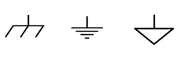
EMC stands for Electromagnetic Compatibility. It refers to the ability of electronic devices and systems to operate properly in their intended electromagnetic environment without causing or experiencing interference. EMC ensures that devices can function without adversely affecting other devices nearby or being affected by electromagnetic interference from external sources. Generally, the ground planes will showing three shapes, please see as following:
Why A Grounding Must be Designed in PCB?
Grounding can be understood as an equipotential point or plane serving as the reference potential for a circuit or system, which can be a specific ground layer in a PCB or the metal chassis of a product. While many perceive the purpose of designing a ground plane primarily to prevent external electromagnetic interference (EMI), but in printed circuit board design, it serves multiple purposes beyond this.
Generally, a well-designed ground provides a common reference zero potential for all circuit units within a system, ensuring no potential difference between circuits and thus stable operation. It also protects circuits from damage, ensuring the safe functioning of electronic products. For instance, ground can provide discharge paths for transient disturbances and dissipate accumulated charges on product metal enclosures induced by static electricity, to prevent potential sparks that may cause interference internally. Additionally, choosing appropriate grounding for shielding structures can yield effective electromagnetic shielding.
Grounding design is very necessary especially for medical industry. As we know, there are many medical devices are directly connected to patients’ bodies, such as monitors. In cases where the chassis carries voltage due to poor grounding, fatal risks may arise. Furthermore, grounding reduces common-mode interference currents flowing through PCBs and prevents high-frequency EMI signals within products from reaching equivalent radiating antennas. Thus, grounding is typically a primary method for noise suppression and interference prevention.
Design Principles of Ground Plane in PCB
A well-designed grounding system should not only consider the radiation and conduction of individual PCBs but also prevent from a systemic perspective. In the design phase, failure to carefully consider the grounding system may indicate a high likelihood of EMC failure for the system. So, knowing the design principles is extremely important to make sure the successful of EMC.
Keep it short and wide
To reduce the impedance of circuits, especially in high-frequency circuits, the ground plane should be made as short and wide as possible. This helps to minimize the return path of the current, thereby reducing EMI.
Partition layout
For complex PCB designs like multilayer PCBs, it is recommended to use a partition layout to separate the ground planes of different functional modules. This helps to isolate noise interference between different modules.
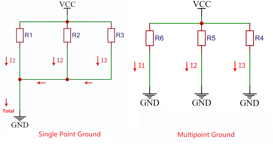
Single-point ground and multipoint ground
Depending on the circuit’s operating frequency and signal characteristics, choose between single-point grounding or multipoint grounding. Single-point grounding is suitable for low-frequency circuits, while multipoint grounding is more suitable for high-frequency circuits.
Ground plane
Where possible, use a ground plane as the ground. The ground plane can provide a low-impedance return path and aid in electromagnetic shielding.
How to Optimize Your Grounding Design?
As for PCB that has already design the circuit layout, how to optimize the ground to get the maximum EMI? Here are some tips that may helpful for you.
Fill the blank areas of the PCB with ground planes to increase the ground plane’s area and reduce impedance.
Reducing the area of ground loops helps to decrease electromagnetic radiation and induced noise.
Power lines and ground planes should be placed as close as possible and run parallel to reduce the area of the current loop.
Placing decoupling capacitors between power and ground planes helps to filter out high-frequency noise.
In PCB EMC design, ground plane design is an essential step that cannot be ignored. By following the principles and optimization methods of ground plane design, the EMC and signal integrity of electronic products can be significantly improved. Therefore, in PCB design, sufficient attention and consideration must be given to ground plane design. Welcome to contact EBest Circuit (Best Technology) if you want to know more about ground and EMC design.