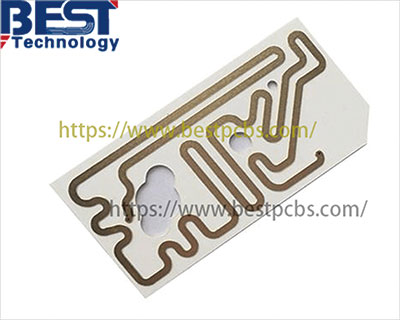
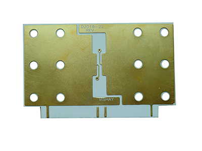
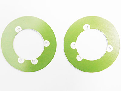
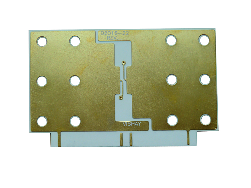
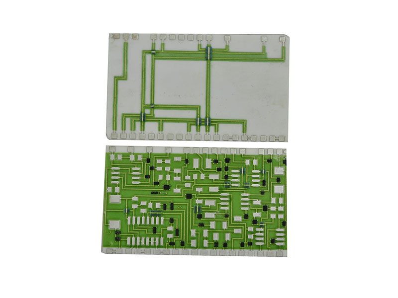
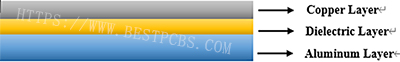
The primary advantage of ceramic multilayer PCBs lies in their thermal properties. The most significant of these is thermal conductivity, which outperforms traditional materials by a tremendous margin. In the table below, the most used board material, FR4, is compared with the ceramic multilayer board in a number of important categories.
MULTILAYER PCB MATERIAL COMPARISON
| Ceramic | Versus | FR4 |
| 28 – 280 | Thermal Conductivity (Wm-K) | 0.8 – 1.1 |
| Component Comparable | Coefficient of Thermal Expansion (CTE) | Component Comparable |
| High | Frequency Performance | Low – Mid |
| Fragile | Handling | Easy |
| Low | Availability | High |
| Mid – High | Cost | Low – Mid |
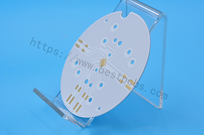
As shown above, ceramic multilayer PCBs have advantages and disadvantages as compared to FR4. However, the advantages point to a continued increase in the use of ceramic boards for high-speed and high-power applications that are criteria for more functionality in smaller packages.
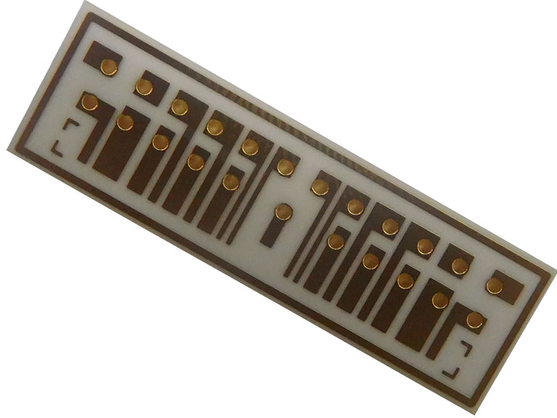
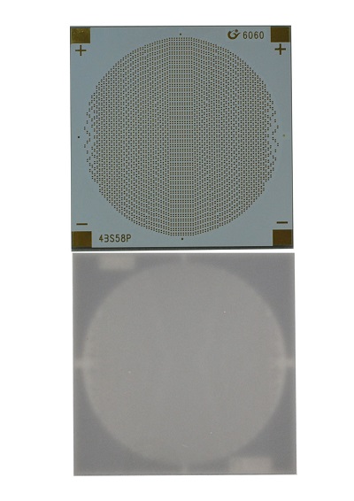
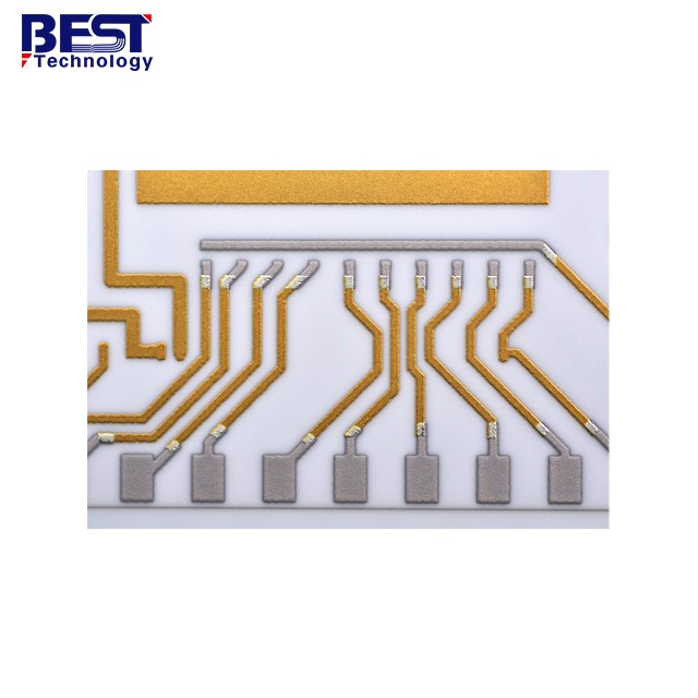
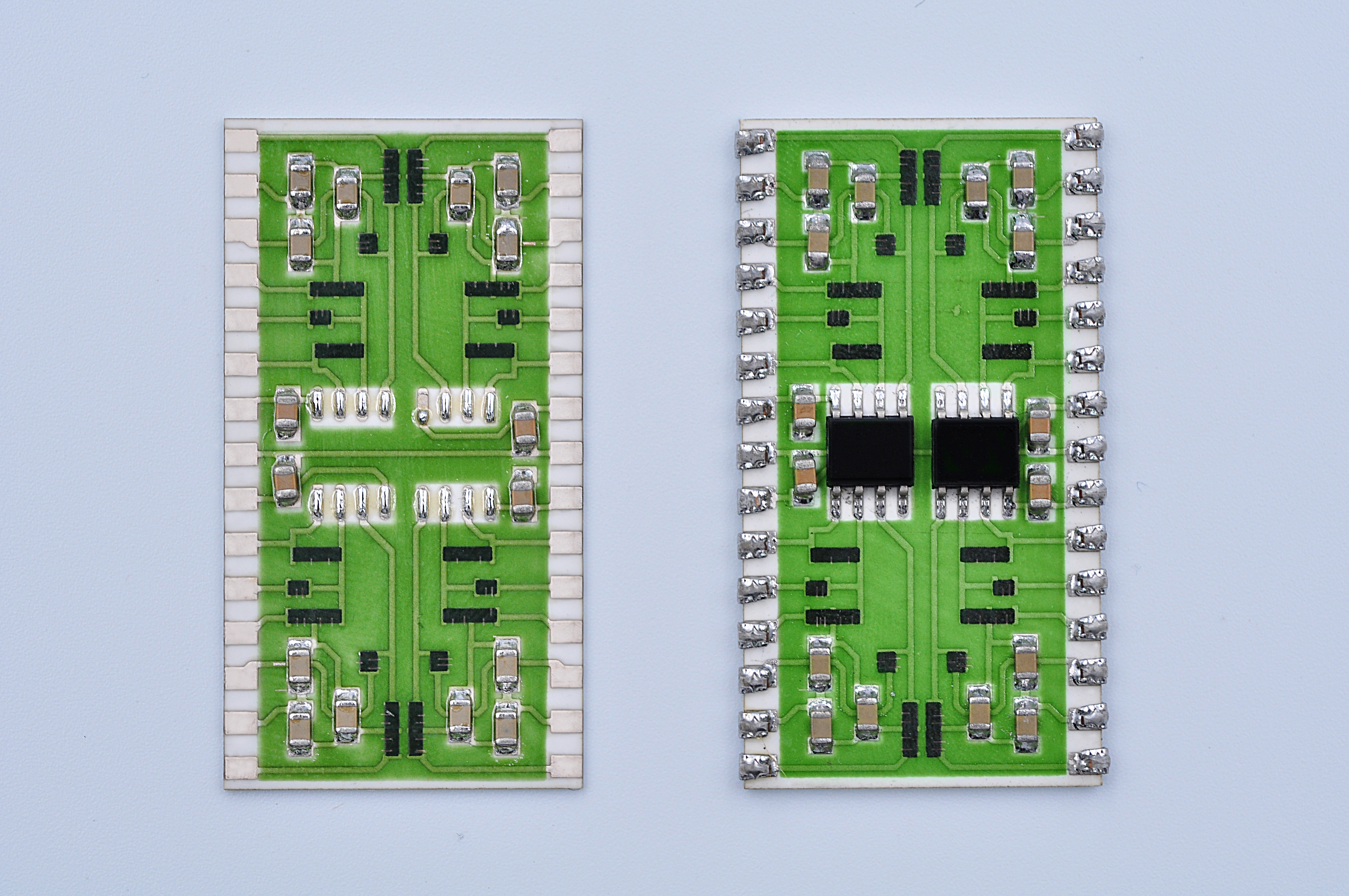
Best Technology, the industry leader in fast, precision and high-quality PCB manufacturing, has a wide range of material options including to meet your design objectives. This includes accommodating the special process of using ceramic materials for your board if desired. We also strive to provide you with the best manufacturing experience.
Best Technology’s Custom PCB Manufacturing Service
1.ISO-9001commitment to quality certifications.
2.Accurate quote in less than 1 day.
3.Performs entire turnkey process in as fast as 3 days.
4.Sources components from the most reputable suppliers in the industry to reduce procurement time.
5.Performs multiple automated inspections during assembly to ensure PCB quality for prototyping.
6.Provides support throughout the PCB manufacturing process, beginning with design.
7.Smooth transition from prototyping to production.