Archive for the ‘Ceramic PCB’ Category

Pros and Cons of the Ceramic PCB

Friday, May 27th, 2022

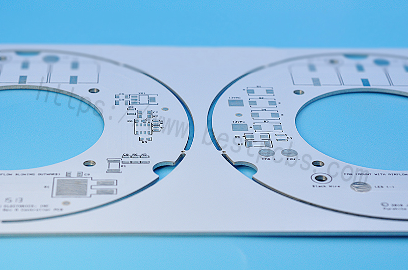
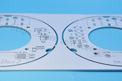
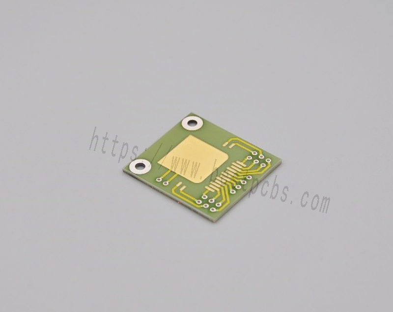
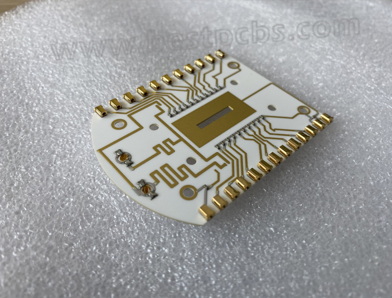
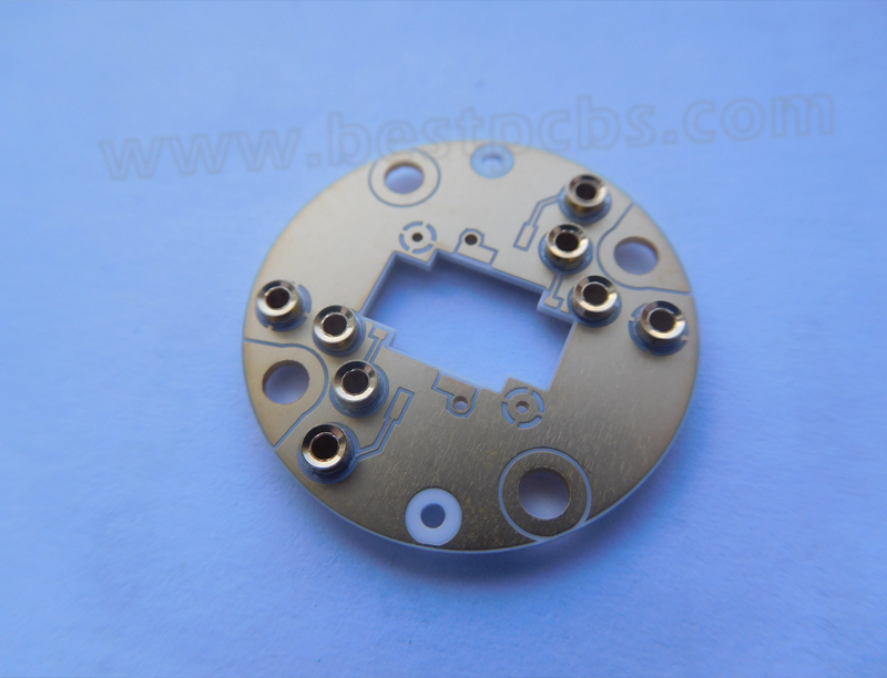
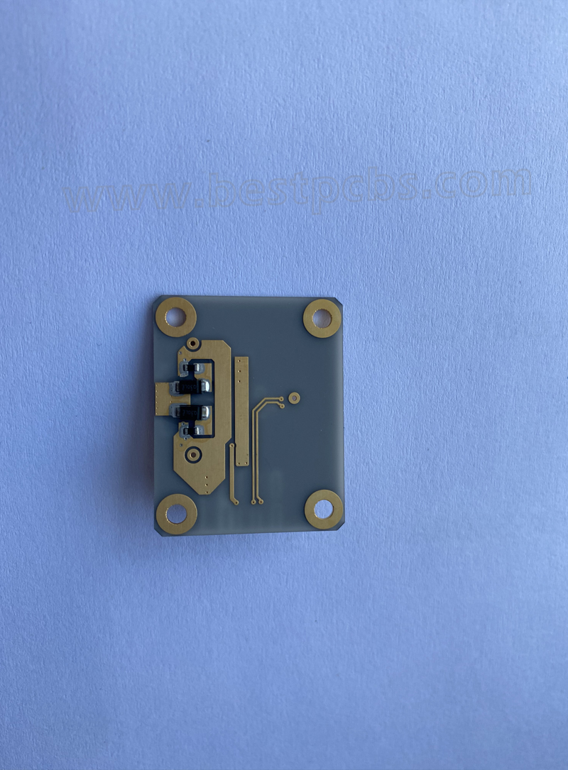
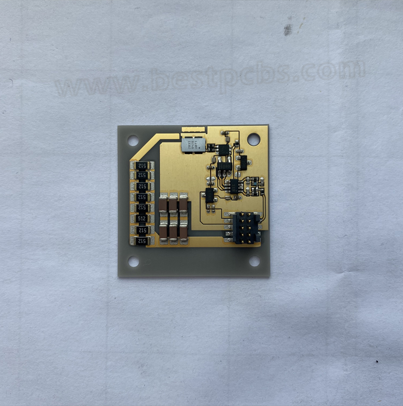
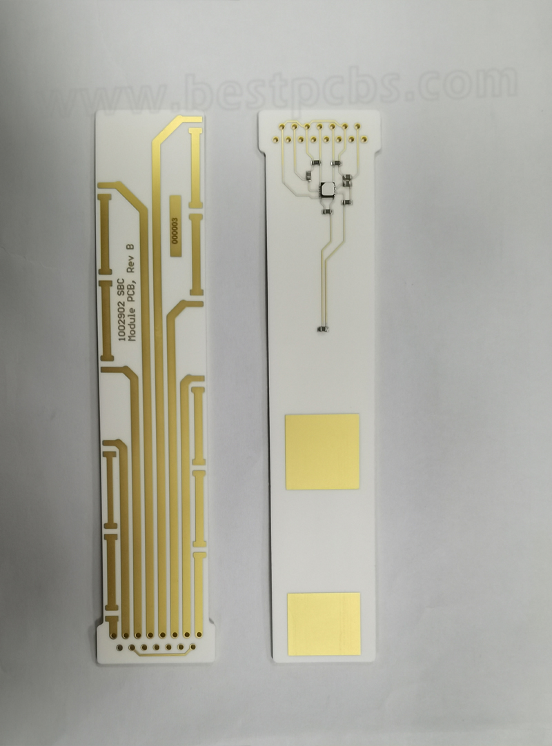
Ceramic PCB is used in various fields because of its high-quality thermal and mechanical advantages. The board’s unique features and high thermal conductivity have enabled it to be used in devices big and small. But meanwhile, it is not flawless. There are also some disadvantages.

Ceramic PCB

Pros of ceramic PCB

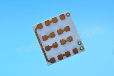
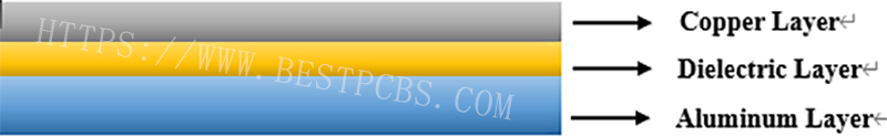
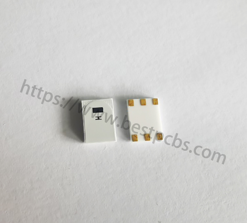
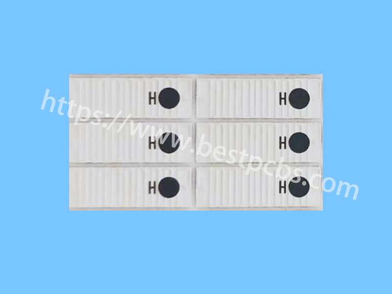
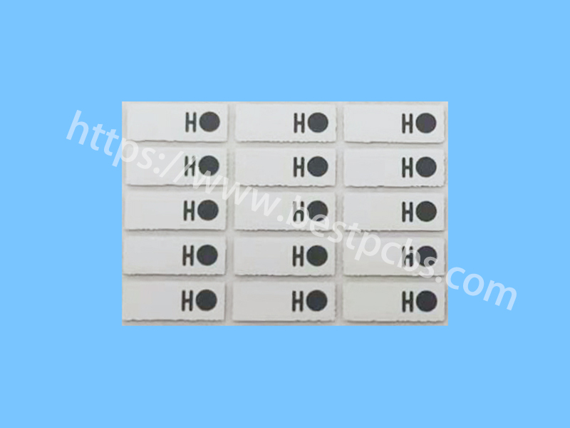
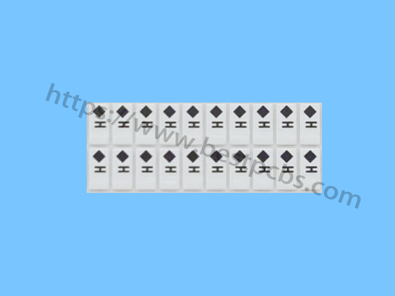
It is supposed that you are familiar with the features below that the ceramic PCB has.

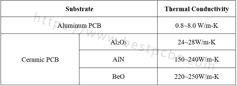
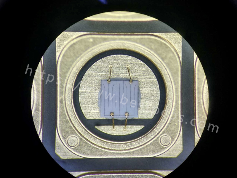
  • Excellent thermal conductivity.
  • Good insulation.
  • High temperature resistance.
  • Great mechanical properties.
  • Compatible with CTE (Coefficient of Thermal Expansion) of components.
  • High-density assembly possible.
  • Non-toxic, conducive to environmental protection.

Cons of ceramic PCB

There are also a few disadvantages that can be found in ceramic PCB. Some of the disadvantages are stated below.

  • Cost—It has a higher cost compared to other printed circuit boards.
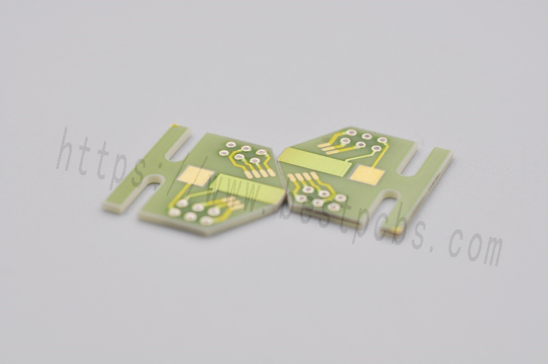
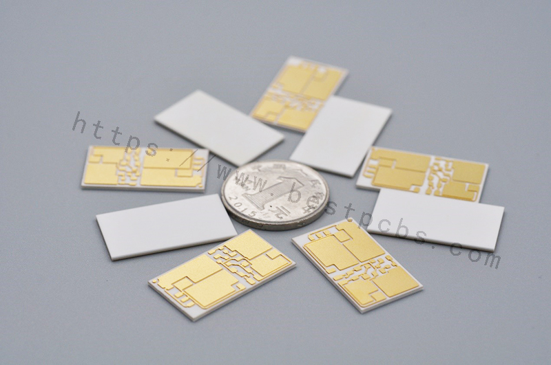
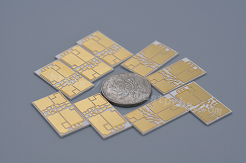
  • Handling—Since ceramic is fragile, it entails careful handling. As ceramic PCB is made for tight spaces, it is very small and this makes it even harder to handle.
  • Availability—It is not as widely available.

Everything has two sides. And ceramic PCB has no exception. But if considering all the advantages and disadvantages, ceramic PCB still takes the win amongst all other boards.

So, this is the end of the article about the advantages and disadvantages of the ceramic PCB. In case if you have any other questions about ceramic PCB or MCPCB, you are welcome to contact us via email at sales@bestpcbs.com. We are fully equipped to handle your PCB or MCPCB manufacturing requirements.

You may also like

Thermal Conductivity—Aluminum PCB vs Ceramic PCB Series 2

Tuesday, April 19th, 2022

Last time we have talked about the structure difference between the aluminum PCB and ceramic PCB. So, based on the different structures, whose thermal conductivity is better?

We have known that a single layer aluminum PCB is made up of copper layer, dielectric layer and aluminum layer. Meanwhile, the dielectric layer is the decisive factor affecting the thermal conductivity.

Generally, its thermal conductivity ranges from 0.8 to 3.0 W/m-K, but can up to 8.0 W/m-K. So, in terms of heat dissipation, the aluminum substrate does much better than FR-4 substrate. And it is a good choice for LED lighting products with high power.

Aluminum PCB

However, the heat-conducting property of ceramic PCB is superior to that of the aluminum PCB.

Since ceramic itself is an insulating material with a great heat-conducting property, it does not need a dielectric layer. Therefore, the heat can be dissipated directly through the ceramic.

Because of its excellent performance in heat dissipation, it is particularly suitable for the lighting product with ultra high power and those products which have a high demand of heat dissipation.

Ceramic PCB

To summarize, clearly, we can know from the table below that ceramic PCB does better than aluminum PCB in terms of thermal conductivity and heat dissipation. And this is mainly because of the dielectric layer, which is related to the functions of bonding, insulation and heat conduction.

The better the heat conduction performance of the insulating layer, the more conducive it is to the diffusion of heat generated during the operation to the device, hence it will be more conducive to lower the operating temperature of the device. That is to say, aluminum PCB will be subject to the dielectric layer, while ceramic PCB will not be restricted.    

And, this is the end of the comparison of the thermal conductivity between aluminum PCB and ceramic PCB. If you still have any questions about them, please feel free to contact us.

You may also like

Differences in Structure——Aluminum PCB vs Ceramic PCB Series 1

Monday, March 21st, 2022

It is supposed that we are familiar with both aluminum PCB and ceramic PCB. But if juxtaposing them, which one will be better by one tally? So, we are about to talk about some differences between them in terms of structure.

Aluminum PCB

Aluminum substrate namely uses aluminum as substrate, which has a good heat dissipation capacity. Generally, it is single-sided, and also can be double-sided while multi-layer aluminum PCB is a little bit hard to manufacture. Besides, a single layer aluminum PCB is made up of copper layer, dielectric layer and aluminum layer.

Structure of Aluminum PCB

Ceramic PCB

Ceramic PCB namely uses ceramic as substrate. Apart from the material, the structure is the biggest difference between ceramic PCB and aluminum PCB. Since ceramic itself is an insulating material, it does not need a dielectric layer. Its structure is as follows.

Structure of Ceramic PCB

Therefore, whether there is a dielectric layer is the main difference in structure between aluminum PCB and ceramic PCB. And dielectric layer plays an important role in thermal conductivity. So, what is the relationship between dielectric layer and thermal conductivity? And whose thermal conductivity is better between aluminum PCB and ceramic PCB?

We will talk about it next time. And if you would like to know the answer, please feel free to contact us, or you can continuously follow our blog site, we will keep updating more information about the differences between aluminum PCB and ceramic PCB on it.

You may also like

Does ceramic PCB is suitable for SMT

Monday, December 20th, 2021

Ceramic PCB is becoming more and more popular due to ceramic PCB with a lot of advantageous performance.

  1. For example, ceramic PCB with good anti-abrasive function because with palladium, the more palladium, anti-abrasive function is better.
  • Ceramic PCB is very good for withstanding high and low temperature too, -55 degree to 850 degrees.
  • Ceramic PCB with great heat dissipation function, ceramic PCB can conduct the heat away very fast and keep the working temperature stable.
  • Ceramic PCB with great heat dissipation function, the thermal conductivity is much better than other PCB, it is very good for high power LED lighting application.

All the ceramic PCB is suitable for SMT, but the SMT is a different from other PCBs, need to control the temperature strictly, and also need to pay high attention to hand it, because ceramic PCB is very fragile, it can be broken very easily.

Please contact sales@bestpcbs.com to know more about ceramic PCB with SMT.

You may also like

Ceramic PCB antennas for Bluetooth sports headset

Thursday, November 11th, 2021

What is the function of the built-in ceramic antenna for the s Bluetooth sports headset?

Ceramic antenna is another miniaturized antenna suitable for Bluetooth devices. The types of ceramic antennas are divided into block-shaped ceramic antennas and multilayer ceramic antennas. The block-shaped antenna is to use high temperature to sinter the whole ceramic body at one time, and then print the metal part of the antenna on the surface of the ceramic PCB.

Ceramic PCB for Bluetooth sports headset

The firing of multilayer antennas by low-temperature co-firing. The multilayer ceramic PCB are laminated and aligned and then sintered at high temperature. Therefore, the metal conductor of the antenna can be printed on each ceramic dielectric layer according to the design needed, which can reduce the size of the antenna size and then can achieve the purpose of hiding the antenna. Since the dielectric constant of the ceramic is higher than other PCB, so using ceramic antennas can effectively reduce the size of the antenna, it is very good for Bluetooth sports headset application. 

Ceramic PCB for Bluetooth sports headset

The material of the ceramic antenna is ceramic, and the weight is only 200g. Its frequency range is between 902MHz and 928MHz. In terms of dielectric loss, the ceramic medium has a smaller dielectric loss than the PCB, so it is in the low power consumption rate. The Bluetooth module is very suitable for it. The effect of the ceramic antenna is stronger than that of the on-board antenna. Generally, there are ANT access feet and ground feet, which are also very convenient to use.

Ceramic PCB for Bluetooth sports headset

The principle of ceramic antennas is divided into two parts: one is the transmitting antenna and the other is the receiving antenna.

  • Porcelain antenna transmitting antenna uses an electrode called “antenna” to turn the high-frequency electric field formed between the antenna and the ground into electromagnetic waves, which can be emitted and propagated to a distance.

Ceramic antenna Receiving antenna uses an electrode called an “antenna” to induce electromagnetic waves from the air into an electric field, generate high-frequency signal voltage, and send it to the receiver for signal processing.

Please feel free to contact sales@bestpcbs.com if you want to know more about ceramic PCB

You may also like

Ceramic PCB is suitable for UVC-LED

Wednesday, September 8th, 2021

Due to COVID-2019, UVC-LED is becoming more and more popular.

The wavelength of UVC-LED is 100-275nm, 265 nm is the best!

Why UVC-LED is becoming more and more popular?

Because UVC-LED has a lot of advantages for sterilization.

High efficiency: The UVC segment ultraviolet light emitted by UVC-LED generally kills bacteria and viruses within a few seconds.

Extensive bactericidal effect: UVC-LED can kill a lot of bacteria.

Safety and environmental protection (without mercury): The most obvious advantage of UVC-LED devices over traditional mercury-excited ultraviolet lamps is that the germicidal light source does not contain mercury or heavy metals, and is simple to operate, safer and more reliable.

Small size, flexible design, easy installation: UVC-LED devices are small in size, and the sterilization device is flexible in design. It can be used in small spaces where traditional ultraviolet mercury lamps cannot be used. It is more in line with the future development trend of high efficiency, small size and integration.

Why ceramic PCB is suitable for UVC-LED?

Because UVC-LED is sensitive to heat.

Due to the low external quantum efficiency (EQE) of UVC-LEDs, only about 1-3% of the input power is converted into light, while the remaining 97% is basically converted into heat. If the heat cannot be dissipated in time and the LED chip is kept below its maximum operating temperature, it will directly affect the service life of the chip, and it may even be unusable.

Due to the small size of UVC-LED, most of the heat cannot be dissipated from the surface, so the back of the LED becomes the only way to effectively dissipate heat. After years of development, UVC-LED is basically based on a flip-chip solution with a high thermal conductivity aluminum nitride substrate. Aluminum nitride (AlN) PCB made by Best Technology has high thermal conductivity (thermal conductivity 180 W/(mK) ~ 260 W/(mK)), which meets the needs of high heat dissipation of UVC-LED and effectively extends the service life of UVC-LED.

Please feel free to contact sales@bestpcbs.com to know more about ceramic PCB for UVC-LED.

Ceramic PCB for UVC LED
AlN Ceramic PCB

You may also like

Why use ceramic circuit boards

Wednesday, August 11th, 2021

With the continuous upgrading and optimization of electronic products, the PCBs as the carrier of components have also been continuously improved, and ceramic circuit boards have appeared. So, compared with traditional glass fiber (FR-4), aluminum-based and copper-based, what’s the advantages of ceramic PCB?

1. Stable flatness

Ordinary PCB is usually made by bonding copper foil and substrate, and the substrate material is mostly glass fiber (FR-4), phenolic resin (FR-3), aluminum-based, copper-based, PTFE, composite ceramics and other materials. The mixture is usually phenolic, epoxy, etc. Due to thermal stress, chemical factors, improper production technology and other reasons during PCB processing, or due to asymmetric copper paving on both sides during the design process, it is easy to cause the PCB board to warp to varying degrees.
The ceramic circuit board is hard with good heat dissipation performance, and low thermal expansion coefficient. At the same time, the ceramic circuit board is bonded to the base material by magnetron/vacuum sputtering. The bonding force is strong and the copper foil will not fall off. High reliability, thus avoiding the

2. Large current carrying capacity:

100A current continuously passes through the 1mm 0.3mm copper board, and the temperature rise is about 17°C; 100A current continuously passes through the 2mm 0.3mm board, and the temperature rise is only about 5°C.

3. Thermal conductivity:

The thermal conductivity of alumina can reach 15~35, and that of aluminum nitride can reach 170~230. Because in the case of high bonding strength, its thermal expansion coefficient will be more matched, and the tested tensile value can reach 45 MPa.

4. Thermal conductivity:

The thermal conductivity of the high thermal conductivity aluminum substrate is generally 1-4W/M. K, and the thermal conductivity of the ceramic substrate can reach about 220W/M. K depending on its preparation method and material formula.

5. Low thermal resistance:

The thermal resistance of a 10—10mm ceramic substrate is 0.63mm thick. The thermal resistance of a ceramic substrate is 0.31K/W, the thermal resistance of a 0.38mm thick ceramic substrate is 0.19K/W, and the thermal resistance of a 0.25mm thick ceramic substrate is 0.14K /W.
 

6. Good insulation performance, high pressure resistance, protection of personal safety and equipment, strong bonding force, bonding technology, copper foil will not fall off, high reliability, stable performance in high temperature and high humidity environments.

7. Stable high-frequency performance, AK and DK values are lower than its PTFE, in line with ceramics.

In summary, with its advantages, ceramic circuit boards have been used in high-power power electronic modules, solar panel components, high-frequency switching power supplies, solid state relays, automotive electronics, aerospace, military electronics, high-power LED lighting products, and communications Antennas, automotive sensors, refrigeration sheets and other fields are widely used.

DSC-1135
DSC-1186

You may also like

Laser drilling and cutting in the production process of ceramic circuit boards

Monday, July 12th, 2021

In the ceramic circuit board processing and production process, laser processing mainly includes laser drilling and laser cutting.

Ceramic materials such as alumina and aluminum nitride have the advantages of high thermal conductivity, high insulation and high temperature resistance, and have a wide range of applications in the fields of electronics and semiconductors. However, ceramic materials have high hardness and brittleness, and its molding and processing are very difficult, especially the processing of micropores. Due to the high power density and good directivity of the laser, lasers are generally used to perforate ceramic plates. Laser ceramic perforation generally uses pulsed lasers or quasi-continuous lasers (fiber lasers). The laser beam is focused on On the workpiece placed perpendicular to the laser axis, a laser beam with high energy density (105-109w/cm2) is emitted to melt and vaporize the material. An air stream coaxial with the beam is ejected by the laser cutting head to remove the melted material from The bottom of the incision is blown out to gradually form a through hole.

Due to the small size and high density of electronic devices and semiconductor components, the precision and speed of laser drilling are required to be high. According to the different requirements of component applications, electronic devices and semiconductor components have small size and high density. Due to its characteristics, the precision and speed of laser drilling are required to be high. According to the different requirements of component applications, the diameter of the micro-hole is in the range of 0.05 to 0.2 mm. For lasers used for ceramic precision processing, generally the focal spot diameter of the laser is less than or equal to 0.05mm. Depending on the thickness and size of the ceramic plate, it is generally possible to control the defocus to achieve through-hole punching of different apertures. For through-holes with a diameter less than 0.15mm, drilling can be achieved by controlling the defocus amount.

There are mainly two types method for cutting ceramic PCB: waterjet cutting and laser cutting. Currently, fiber lasers are mostly used for laser cutting. Fiber laser cutting ceramic circuit boards has the following advantages:

(1) High precision, fast speed, narrow cutting seam, small heat-affected zone, smooth cutting surface without burrs.

(2) The laser cutting head will not touch the surface of the material and will not scratch the workpiece.

(3) The slit is narrow, the heat-affected zone is small, the local deformation of the workpiece is extremely small, and there is no mechanical deformation.

(4) The processing flexibility is good, it can process any graphics, and it can also cut pipes and other special-shaped materials.

Al2O3 PCB with drilling
AlN PCB with drilling

 Under the development trend of light and thin, miniaturization, etc., the traditional cutting processing method has not been able to meet the demand due to the insufficient precision. Laser is a non-contact processing tool, which has obvious advantages over traditional processing methods in cutting process, and plays a very important role in the processing of ceramic substrate PCB.

Please contact sales@bestpcbs.com if you want to know more ceramic PCB.

You may also like

The technology and application of DBC ceramic PCB

Thursday, June 17th, 2021

DBC means direct bonding copper, it is a ceramic surface metallization technology.

The copper is bonded on Alumina, Beryllium Oxide and Aluminum Nitride, Packaging applications for power electronic modules, semiconductor refrigeration and LED devices are widely used.

DBC-Ceramic-PCB

96% Al2O3 has good insulation, good chemical stability, high strength, and low price. It is the preferred material for DBC technology, but the thermal conductivity of aluminum oxide is low, and there is a certain thermal mismatch with the thermal expansion coefficient of Si.

BeO is a good ceramic material used in DBC technology. It has high low-temperature thermal conductivity. It can be used for medium and high power devices. In the application field and process, the toxicity caused by it should be properly protected.

AlN material is non-toxic, moderate dielectric constant, thermal conductivity is much higher than aluminum oxide, close to beryllium oxide, and thermal expansion coefficient close to SI. All kinds of chips and high-power devices can be directly attached to the AlN substrate. No transition layer of other materials is used. The prospects currently used in DBC technology are very promising.

There is no any layer between the metal and ceramic substrate, so the thermal diffusion ability is strong; the contact resistance is also low, which is conducive to the connection of high-power and high-frequency devices.     

The linking temperature is lower than the melting point of copper, and the DBC substrate maintains a stable geometric shape during the connection process. In some cases, the copper foil can be made into the required shape before the linking, and then the DBC preparation process is performed, eliminating the need After connecting the etching process.

The copper conductor part has a very high current-carrying capacity, so it has the ability to reduce the size of the intercepting medium and increase the power capacity.

If you want to know more about DBC ceramic PCB, please feel free to contact sales8@bestpcbs.com

You may also like

How to do SMT for ceramic PCB

Wednesday, May 19th, 2021

As we all know if ceramic PCB is very fragile, so it is not easy to do SMT for them.

But we can do the SMT for ceramic PCB easily because we do it every day and we have more than 15 years experiences for doing that.

For the almost SMD components (such as SMD rsistors, capacitors, diode etc), normally we will add the solder paste by using SMT stencil, then put the components by machine, finally do the oven reflow.

For some special components, we will need to solder it by hand, such as through connectors, but it can’t be soldered by hand directly, it need to be put on the heating table to keep the temperature is high enough to make the solder past at melt state. Because the ceramic material with very good heat dissipation, the solder paste will be solidification very easily if don’t put the ceramic PCB on heating table

For some small LED, it can’t be put by SMT machine, because no such small feeder to pick it up, then need to put it on board by hand.

We can do very well for the small BGA components too.

Below some photos of ceramic PCB.

If you would like to know more about ceramic and ceramic PCB SMT, please feel free to email me

Ceramic PCB with SMT 1
Ceramic PCB with SMT 2
Ceramic PCB with SMT 3
Ceramic PCB with SMT 4
Ceramic PCB with SMT 5

You may also like