PCB manufacturing PCB manufacturing
Home > Blog

Sheet Metal Fabrication Services for Custom Industrial Parts

June 3rd, 2026

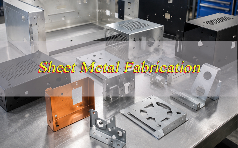
Sheet metal fabrication is the process of cutting, bending, forming, welding, and finishing metal sheets into custom parts, enclosures, brackets, panels, frames, and industrial components. It is widely used in electronics, machinery, automotive, medical equipment, energy systems, communication devices, and industrial control products. A successful project depends on the right material, manufacturable design, accurate tolerances, stable finishing, and a supplier that can support both prototypes and batch production.

Sheet Metal Fabrication, https://www.bestpcbs.com/blog/2026/06/sheet-metal-fabrication/

What Is Sheet Metal Fabrication?

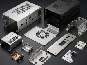
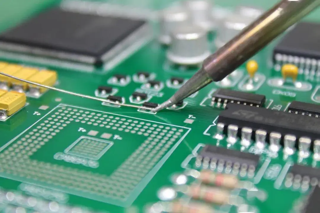
Sheet metal fabrication is a manufacturing method that turns flat metal sheets into functional parts through cutting, punching, bending, welding, riveting, hardware insertion, surface treatment, and assembly. The process is suitable for both simple brackets and complex enclosures with holes, louvers, PEM fasteners, hinges, grounding points, and mounting features.

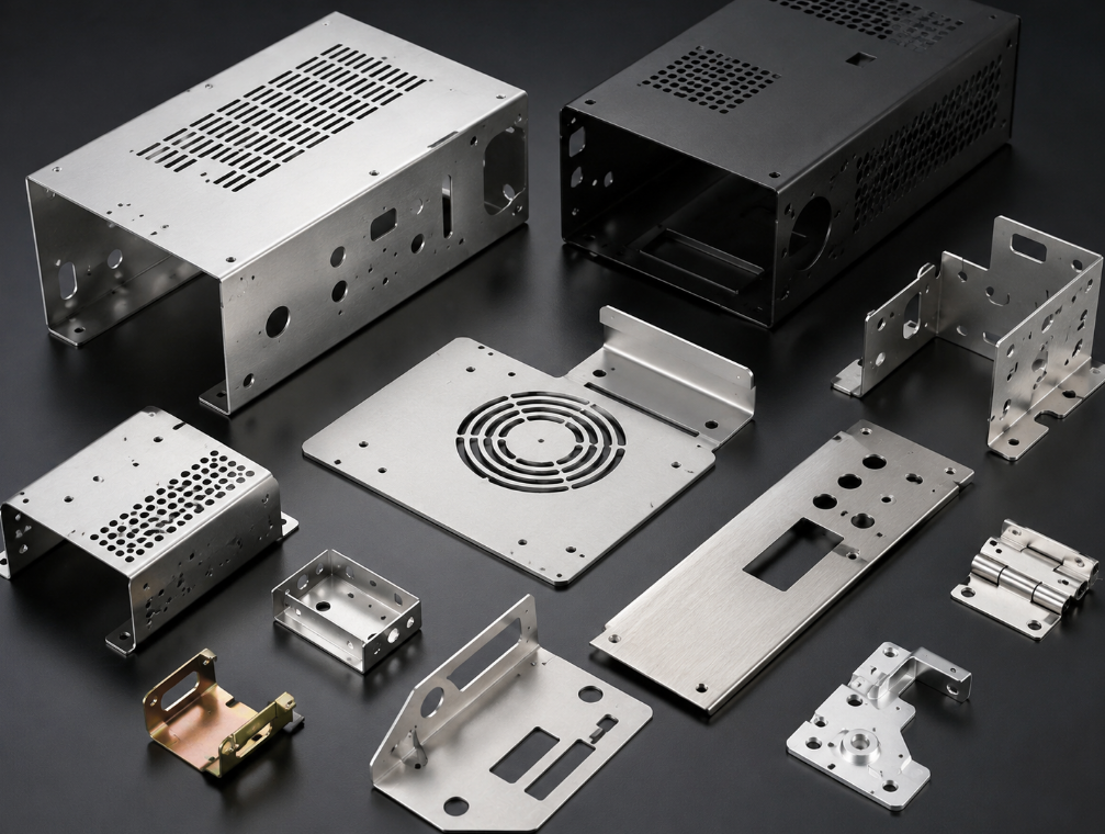
Common sheet metal parts include electronic enclosures, machine covers, control cabinets, chassis, mounting brackets, shielding covers, battery boxes, telecom housings, medical equipment panels, and industrial frames. Compared with machining from solid blocks, sheet metal fabrication can reduce material waste and support faster production for many structural parts.

For B2B projects, sheet metal fabrication is not only about shaping metal. It also involves engineering review, tolerance control, material selection, surface finishing, cost optimization, quality inspection, and reliable delivery.

Why Is Sheet Metal Fabrication Important for Industrial Projects?

Sheet metal fabrication is important because many industrial products need strong, lightweight, protective, and cost-controlled metal structures. A well-designed fabricated part can protect internal components, improve heat dissipation, support assembly accuracy, and extend product life.

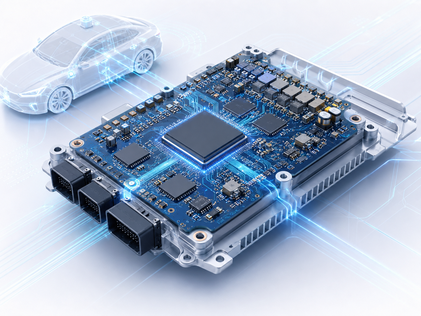
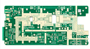
In electronics and PCB-related projects, sheet metal fabrication is often used for control boxes, server chassis, power supply enclosures, communication housings, shielding covers, test fixtures, and box-build assemblies. EBest provides PCB design, PCB prototype, mass production, component sourcing, PCB assembly, and box-build assembly services, making fabricated enclosures and electromechanical integration especially relevant for complete product builds.

For buyers, sheet metal fabrication also affects project cost, lead time, compliance, logistics, and after-sales stability. Poor bending design, wrong material thickness, weak welding, or unsuitable coating may cause rework, assembly failure, corrosion, or field complaints.

How Does Sheet Metal Fabrication Work?

Sheet metal fabrication usually starts from engineering files such as 2D drawings, 3D CAD files, DXF files, STEP files, BOM lists, and finishing requirements. The supplier reviews material grade, thickness, bend radius, hole position, tolerance, coating, fasteners, and assembly requirements before production.

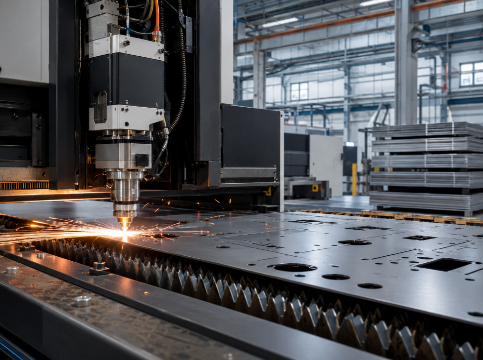
A typical workflow includes material preparation, laser cutting or punching, deburring, bending, welding or riveting, hardware insertion, surface finishing, inspection, packing, and shipment. For complex projects, prototype validation is often used before mass production to confirm fit, appearance, function, and assembly compatibility.

The key is process matching. Laser cutting is suitable for flexible custom shapes, punching is efficient for repeated holes, bending forms the structure, welding connects parts, and finishing protects the surface. Each step must match the final use environment.

What Are the Main Types of Sheet Metal Fabrication Services?

Sheet metal fabrication services can be divided by process, product type, and production volume. The most common services include laser cutting, CNC punching, CNC bending, stamping, welding, riveting, hardware insertion, grinding, polishing, powder coating, anodizing, plating, and assembly.

Prototype sheet metal fabrication is used for engineering samples, functional testing, new product development, and low-volume trial orders. It focuses on speed, flexibility, and design verification.

Custom sheet metal fabrication is used when parts require unique dimensions, special holes, brand-specific enclosures, functional brackets, or project-specific mounting structures.

Precision sheet metal fabrication focuses on tighter tolerances, clean edges, stable bending angles, and consistent assembly fit. It is common in electronics, medical devices, telecom equipment, and industrial automation.

Mass production sheet metal fabrication focuses on repeatability, cost control, stable quality, and predictable delivery.

What Materials Are Used in Sheet Metal Fabrication?

The right material depends on strength, weight, corrosion resistance, conductivity, appearance, cost, and working environment. Different materials behave differently during cutting, bending, welding, and finishing.

MaterialCommon AdvantagesTypical ApplicationsKey Notes
Cold-rolled steelGood strength, stable forming, lower costCabinets, brackets, chassis, panelsUsually needs coating or plating
Stainless steelCorrosion resistance, clean appearance, high durabilityMedical devices, food equipment, outdoor partsHarder to process than mild steel
AluminumLightweight, corrosion resistance, good appearanceEnclosures, panels, telecom housingsGood for anodizing and weight reduction
Galvanized steelBetter corrosion resistance than plain steelCovers, HVAC parts, industrial boxesWelding may affect zinc coating
CopperHigh conductivity, thermal performanceElectrical parts, grounding, shieldingHigher material cost
BrassGood appearance, corrosion resistance, machinabilityDecorative panels, terminals, fittingsUsed when appearance or conductivity matters

For electronic enclosures and PCB-related assemblies, aluminum and stainless steel are common choices when weight, corrosion resistance, shielding, or appearance matters. Cold-rolled steel is often selected when cost and strength are more important.

What Sheet Metal Fabrication Processes Are Commonly Used?

The most common sheet metal fabrication processes include cutting, punching, bending, welding, hardware insertion, and finishing. Each process affects final quality and cost.

ProcessFunctionBest Used ForQuality Focus
Laser cuttingCuts flat profiles from sheet metalCustom shapes, prototypes, small batchesEdge quality, heat marks, dimensional accuracy
CNC punchingCreates holes, slots, louvers, formsRepeated features, batch productionTooling marks, hole spacing, burr control
CNC bendingForms angles and flangesEnclosures, brackets, framesBend angle, radius, springback
WeldingJoins separate metal partsFrames, boxes, structural partsStrength, distortion, appearance
RivetingMechanical joiningPanels, brackets, assembliesFastener strength, alignment
PEM insertionAdds threaded hardwareEnclosures, mounting pointsPull-out strength, position accuracy
Powder coatingProtective and decorative finishSteel enclosures, outdoor equipmentAdhesion, color, thickness
AnodizingProtective finish for aluminumPanels, housings, visible partsColor consistency, surface marks
PlatingConductive or anti-corrosion finishElectrical parts, terminalsCoating thickness, adhesion

Laser cutting and CNC bending are widely used in custom sheet metal fabrication because they support flexible design changes without expensive tooling. Stamping may be better for very high-volume production after the design is finalized.

Sheet Metal Fabrication Process, https://www.bestpcbs.com/blog/2026/06/sheet-metal-fabrication/

What Design Rules Matter in Sheet Metal Fabrication?

Good sheet metal design should consider bending, hole spacing, minimum flange length, bend relief, material thickness, and tolerance stack-up. Design mistakes can increase cost or cause cracking, distortion, misalignment, and assembly problems.

A common design rule is to keep the inside bend radius at least equal to the material thickness when possible. This helps reduce cracking and distortion during forming. Flange length should also be long enough for stable bending and repeatable forming.

Holes should not be placed too close to bend lines, because bending can deform nearby features. For critical holes, slots, connectors, and mounting points, designers should confirm bend allowance, bend deduction, and tolerance requirements before releasing drawings.

Uniform material thickness is also important. Sheet metal parts are usually made from one sheet thickness, so sudden wall thickness changes are not practical in the same way they might be in casting or machining.

What Tolerances Are Used in Sheet Metal Fabrication?

Sheet metal tolerances depend on material type, thickness, part size, cutting method, bending complexity, welding distortion, finishing thickness, and inspection method. General tolerances may be enough for non-critical covers, while tighter tolerances are needed for connectors, mounting holes, hinges, and assembly interfaces.

ISO 2768 is commonly used as a general tolerance reference for linear and angular dimensions when drawings do not specify individual tolerances. It helps reduce ambiguity between buyer and manufacturer.

FeatureCommon Tolerance ConcernPractical Suggestion
Overall length and widthCutting accuracy and material movementDefine critical and non-critical dimensions
Hole positionAssembly fit, screw alignment, connector matchAdd tighter tolerance only where needed
Bend angleSpringback and press brake setupConfirm acceptable angular tolerance
FlatnessWelding, heat, coating, sheet stressAvoid over-tight flatness unless required
Threaded insertsPull strength and positionSpecify hardware type and load requirement
Coating thicknessFit, grounding, appearanceMask threads or contact areas if needed

For cost control, do not apply tight tolerances to every feature. Mark only functional dimensions as critical, and allow standard tolerances for non-functional areas.

How Is Sheet Metal Fabrication Different from CNC Machining and Stamping?

Sheet metal fabrication, CNC machining, and stamping can all make metal parts, but they are suitable for different project needs.

MethodBest ForAdvantagesLimitations
Sheet metal fabricationEnclosures, panels, brackets, coversGood cost, fast prototypes, flexible designLimited by bend rules and sheet thickness
CNC machiningSolid metal parts, precision blocks, complex 3D featuresHigh precision, strong geometry controlMore material waste, higher cost for large covers
StampingHigh-volume repeated partsVery fast unit production, low cost at scaleTooling cost, less flexible for design changes

Sheet metal fabrication is often the best choice for custom industrial covers, control boxes, chassis, racks, brackets, and electronic enclosures. CNC machining is better for high-precision solid parts. Stamping is better when the design is stable and production volume is high enough to justify tooling.

What Surface Finishes Are Available for Sheet Metal Parts?

Surface finishing improves corrosion resistance, appearance, insulation, conductivity, and product lifetime. The right finish depends on material, environment, visual requirements, and assembly function.

FinishSuitable MaterialsMain PurposeNotes
Powder coatingSteel, aluminumCorrosion protection and colorDurable, common for enclosures
AnodizingAluminumCorrosion resistance and appearanceGood for panels and housings
Zinc platingSteelAnti-corrosion protectionCommon for brackets and hardware
Nickel platingSteel, copper alloysConductivity and corrosion resistanceUsed for functional surfaces
BrushingStainless steel, aluminumDecorative appearanceVisible grain direction
PolishingStainless steel, aluminumSmooth appearanceHigher labor cost
PassivationStainless steelImprove corrosion resistanceUsed for clean and medical parts
PaintingSteel, aluminumColor and protectionRequires surface preparation

For electronic products, grounding and conductivity must be considered. Powder coating may insulate surfaces, so grounding points, screw holes, or contact areas may need masking.

What Common Defects Should Be Avoided in Sheet Metal Fabrication?

Common sheet metal fabrication defects include burrs, scratches, wrong hole position, bending cracks, angle deviation, warping, welding distortion, weak welds, poor coating adhesion, color mismatch, and threaded insert failure.

Burrs may affect assembly safety and appearance. Scratches may be unacceptable for visible panels. Wrong hole position can cause connector mismatch. Welding distortion can make assemblies difficult to install. Poor coating adhesion may lead to peeling, corrosion, or customer complaints.

Many defects are preventable through engineering review, proper bend radius, correct cutting parameters, deburring, welding sequence control, surface preparation, coating thickness control, and final inspection. For batch production, first article inspection is especially important before full production starts.

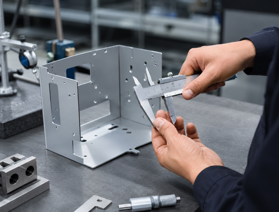
What Quality Control Is Needed for Sheet Metal Fabrication?

Quality control should cover incoming material, cutting dimensions, bending angles, welding strength, hardware insertion, surface finishing, assembly fit, packaging, and final inspection. For industrial and electronic projects, inspection should not focus only on appearance. Fit, function, grounding, protection, and installation reliability are equally important.

Common inspection methods include caliper measurement, height gauge inspection, angle gauge checking, coating thickness testing, visual inspection, assembly trial fitting, pull-out testing for inserts, salt spray testing for corrosion resistance, and packaging drop-risk review.

EBest has long-term manufacturing experience and supports industrial quality systems including ISO 9001:2015, IATF 16949, ISO 13485:2016, AS9100D, REACH, RoHS, and UL-related compliance capabilities.

Sheet Metal Fabrication, https://www.bestpcbs.com/blog/2026/06/sheet-metal-fabrication/

What Factors Affect Sheet Metal Fabrication Cost?

Sheet metal fabrication cost is affected by material type, thickness, part size, cutting length, number of holes, bending times, welding length, finishing method, tolerance level, order quantity, packaging, and delivery requirements.

Cost FactorWhy It MattersHow to Control Cost
MaterialStainless steel and copper usually cost moreSelect material by function, not habit
ThicknessThicker sheets take more cutting and bending forceAvoid over-designing thickness
Cutting complexityMore holes and curves increase processing timeSimplify non-functional features
Bending timesEach bend adds setup and process timeReduce unnecessary bends
WeldingLabor-intensive and may need grindingUse tabs, rivets, or fasteners when suitable
Surface finishPowder coating, anodizing, plating add costChoose finish by environment
TolerancesTight tolerance increases inspection and rework riskTighten only critical dimensions
QuantitySmall batches have higher unit setup costCombine orders when possible

A good supplier should help optimize the design instead of only quoting from drawings. Small changes in hole layout, flange size, welding method, or coating requirement can reduce cost without reducing performance.

Where Is Sheet Metal Fabrication Commonly Used?

Sheet metal fabrication is used across many industries because it offers strength, customization, scalability, and cost efficiency.

Electronics and PCB assemblies use sheet metal enclosures, shielding covers, control boxes, racks, and chassis.

Industrial automation uses brackets, machine covers, control panels, frames, and safety guards.

Medical equipment uses stainless steel panels, device housings, carts, covers, and cleanable structures.

Telecom and communication equipment uses server chassis, RF housings, base station covers, and network equipment enclosures.

Automotive and EV systems use battery boxes, brackets, sensor housings, mounting plates, and protective covers.

Energy and power systems use inverter enclosures, power distribution boxes, solar equipment brackets, and control cabinets.

What Files Are Needed for a Sheet Metal Fabrication Quote?

A clear quotation needs complete engineering information. Missing files or unclear requirements often cause inaccurate pricing, repeated communication, and production delays.

Required File or InformationPurpose
2D drawingDefines dimensions, tolerances, notes, finish, inspection points
3D CAD fileHelps review bending, assembly, interference, and structure
Material gradeConfirms strength, corrosion resistance, and forming behavior
ThicknessAffects bending, cutting, weight, and cost
Surface finishDefines coating, color, texture, corrosion protection
QuantityAffects unit price, setup cost, and production method
Critical dimensionsHelps supplier control functional features
Assembly requirementsConfirms PEM inserts, welding, riveting, hinges, seals
Application environmentHelps choose material and finish
Packing requirementsPrevents scratches, deformation, and shipping damage

STEP, DXF, DWG, PDF, and BOM files are commonly used. For enclosure projects, connector drawings, PCB assembly drawings, and internal clearance requirements are also useful.

How to Choose a Reliable Sheet Metal Fabrication Supplier?

A reliable sheet metal fabrication supplier should understand engineering, manufacturing, quality, finishing, and delivery. Price is important, but the lowest quote may not be the safest choice if it ignores tolerances, coating, welding distortion, or assembly fit.

Check whether the supplier can review drawings, suggest DFM improvements, provide prototype support, control batch quality, manage surface finishing, and pack parts safely for international shipping. For electronic and industrial projects, experience with enclosures, chassis, brackets, grounding, and box-build assembly is especially valuable.

A good supplier should also communicate clearly. They should confirm material grade, finish standard, color code, tolerance level, hardware type, thread specification, masking area, and inspection method before production.

Why Choose EBest for Sheet Metal Fabrication Support?

EBest supports customers with one-stop electronic manufacturing solutions, including PCB design, PCB prototype, mass production, component sourcing, PCB assembly, and box-build assembly. For projects that require sheet metal enclosures, panels, brackets, or chassis around PCB assemblies, this integrated service can reduce communication gaps between the circuit board, components, mechanical housing, and final product assembly.

For industrial buyers, this is useful when a project needs more than one part. A PCB may need a metal enclosure, thermal path, mounting structure, grounding design, cable openings, labels, connectors, and final assembly. Coordinating these requirements early can reduce rework and improve project delivery.

EBest can support prototype development, engineering review, production coordination, quality control, and global delivery for customers who need custom electronic and industrial manufacturing solutions.

Sheet Metal Fabrication, https://www.bestpcbs.com/blog/2026/06/sheet-metal-fabrication/

What Should You Check Before Starting a Sheet Metal Fabrication Project?

Before starting production, confirm the part function, installation method, material, thickness, finish, tolerance, quantity, and operating environment. If the part must fit with PCB assemblies, connectors, displays, switches, fans, cables, or fasteners, these interfaces should be checked before manufacturing.

Also confirm whether the drawing has clear bend direction, flat pattern, hole position, thread type, surface finish, color code, critical dimensions, and inspection requirements. For powder-coated or plated parts, coating thickness may affect holes, threads, slots, and grounding areas.

For batch production, make a prototype first when the design is new, complex, or appearance-sensitive. A small verification step can prevent expensive batch rework.

FAQs About Sheet Metal Fabrication

Q1: What is sheet metal fabrication used for?
A1: Sheet metal fabrication is used to make enclosures, brackets, panels, chassis, frames, cabinets, covers, and structural parts. It is common in electronics, industrial automation, medical devices, telecom equipment, automotive systems, energy products, and custom machinery.

Q2: What is the best material for sheet metal fabrication?
A2: The best material depends on the application. Cold-rolled steel is cost-effective, stainless steel offers corrosion resistance, aluminum is lightweight, galvanized steel improves rust protection, and copper is suitable for conductivity or shielding needs.

Q3: Is aluminum good for sheet metal fabrication?
A3: Yes. Aluminum is widely used because it is lightweight, corrosion-resistant, and suitable for anodizing. It is often used for electronic enclosures, panels, communication housings, and products where weight reduction matters.

Q4: What thickness is used for sheet metal parts?
A4: Thickness depends on strength, size, weight, bending, and cost. Thin sheets are used for covers and panels, while thicker sheets are used for structural brackets, cabinets, and load-bearing parts.

Q5: What is the difference between sheet metal fabrication and stamping?
A5: Sheet metal fabrication is more flexible for custom parts, prototypes, and small to medium batches. Stamping is better for high-volume production after tooling is built.

Q6: How can I reduce sheet metal fabrication cost?
A6: You can reduce cost by simplifying part geometry, avoiding unnecessary tight tolerances, choosing suitable material, reducing welding, standardizing hole sizes, and selecting a finish that matches the working environment.

Q7: Why do sheet metal parts crack during bending?
A7: Cracking can happen when the bend radius is too small, the material is too hard, the grain direction is unsuitable, or the design has features too close to the bend. Proper bend radius and material selection help prevent this problem.

Q8: What files should I send for a sheet metal fabrication quote?
A8: Send 2D drawings, 3D CAD files, material grade, thickness, finish, quantity, tolerance requirements, and application details. For enclosures, also provide PCB dimensions, connector positions, cable openings, and assembly requirements.

Q9: Can sheet metal fabrication be used for electronic enclosures?
A9: Yes. Sheet metal fabrication is widely used for electronic enclosures, control boxes, server chassis, power supply housings, shielding covers, and communication equipment cases.

Q10: What surface finish is best for sheet metal enclosures?
A10: Powder coating is common for steel enclosures because it provides color and corrosion protection. Anodizing is common for aluminum parts. Stainless steel may use brushing, polishing, or passivation depending on appearance and environmental requirements.

Q11: How long does sheet metal fabrication take?
A11: Lead time depends on material availability, part complexity, quantity, finishing, and inspection needs. Simple prototypes may be faster, while welded, coated, or assembled parts usually need more time.

Q12: How do I choose a sheet metal fabrication manufacturer?
A12: Choose a manufacturer with engineering review ability, stable process control, suitable equipment, quality inspection, finishing support, clear communication, and experience with your application.

Conclusion

Sheet metal fabrication is a practical manufacturing solution for custom enclosures, brackets, panels, chassis, covers, and industrial structural parts. The best results come from matching material, thickness, tolerance, bend design, finishing, quality control, and supplier capability with the real application.

For buyers and engineers, the safest approach is to confirm the design early, define only the necessary critical tolerances, select materials based on environment and function, and work with a supplier that understands both fabrication and final assembly.

If you need sheet metal fabrication support for electronic enclosures, industrial parts, PCB-related box-build projects, OEM manufacturing, ODM production, sample development, batch production, or custom engineering solutions, you can contact our team at sales@bestpcbs.com for technical support and quotation service.

You may also like

What Is Semi Additive Process? Semi-Additive Process vs Subtractive Etching

June 2nd, 2026

The semi additive process is an advanced PCB fabrication method used to create fine copper traces for HDI boards, ultra-HDI boards, IC substrates, RF modules, and compact electronic devices.

Unlike subtractive etching, which removes unwanted copper from copper foil, this method builds copper only where the circuit pattern is needed. This supports finer line width, tighter spacing, cleaner trace profiles, and better dimensional control.

This guide explains what is semi additive process, how SAP works, where it is used, and how the semi-additive process vs subtractive etching comparison helps select the right circuit formation method for fine-line PCB projects.

Semi Additive Process, https://www.bestpcbs.com/blog/2026/06/semi-additive-process/

What Is Semi Additive Process?

The semi additive process, often called SAP, is a PCB circuit formation method that combines copper plating with limited copper removal. It does not rely mainly on heavy copper etching.

SAP uses a thin seed copper layer as the base. Copper is then selectively plated onto the areas that will become traces, pads, and circuit features.

It is called “semi additive” because copper is added to the required circuit pattern, while only a thin seed layer is removed later. Compared with subtractive etching, this method can produce straighter trace walls, finer spacing, and better dimensional accuracy.

In PCB production, SAP is commonly used for HDI boards, ultra-HDI boards, advanced IC substrates, flexible circuits, and miniaturized electronics. It helps overcome the routing limits of conventional copper foil etching.

What Are the Main Steps of Semi Additive Process?

SAP forms PCB circuits by first creating a thin conductive seed layer. Copper is then selectively plated only where the circuit pattern is required. Compared with subtractive etching, this process removes much less copper. As a result, it can produce finer traces, cleaner line edges, and more stable spacing for advanced fine-line PCB manufacturing.

Step 1: Prepare the dielectric surface
The PCB substrate surface is cleaned and treated to improve copper bonding. This step removes contamination and prepares the surface for seed layer formation.

Step 2: Form a thin seed copper layer
A very thin conductive copper layer is applied to the surface. This seed layer provides the base for later electroplating.

Step 3: Apply photoresist
Photoresist is laminated or coated onto the panel. It works as a temporary mask during circuit pattern formation.

Step 4: Expose and develop the circuit pattern
The required circuit image is exposed onto the photoresist. After development, only the areas that need copper plating remain open.

Step 5: Electroplate copper traces
Copper is plated into the open pattern areas. These plated areas become the final traces, pads, and circuit features.

Step 6: Strip the photoresist
After copper plating, the remaining photoresist is removed from the panel. The plated copper circuit pattern is now exposed.

Step 7: Remove the exposed seed layer
The thin seed copper between traces is removed by flash etching. Because the seed layer is very thin, undercutting is much lower than in subtractive etching.

Step 8: Inspect the finished circuit layer
AOI, copper thickness measurement, adhesion testing, and microsection inspection are used to confirm line width, spacing, copper quality, and process stability.

Semi Additive Process Steps, https://www.bestpcbs.com/blog/2026/06/semi-additive-process/

What Is Modified Semi Additive Process?

The modified semi additive process, or mSAP, is a variation of SAP used in advanced PCB production. It is suitable when a circuit needs finer line width and spacing than standard subtractive etching can support.

In mSAP, production usually begins with thin copper foil or an ultra-thin copper layer. Copper is selectively plated to form the circuit pattern, and the exposed base copper is then removed.

This method reduces the amount of copper that needs to be etched. It helps create finer traces and more vertical trace profiles than traditional subtractive fabrication.

mSAP is widely used in smartphones, wearable devices, advanced modules, communication equipment, and compact PCB designs. It offers a balance between fine-line capability, production scalability, cost, and manufacturability.

What Is the Difference Between SAP and mSAP?

SAP and mSAP both use selective copper plating to form fine circuit patterns. The main difference is the starting copper layer, fine-line capability, cost, and production suitability.

ItemSAPmSAP
Full nameSemi Additive ProcessModified Semi Additive Process
Starting copper layerExtremely thin seed copper layerThin copper foil or modified base copper
Main process logicBuild copper traces mainly by platingPlate copper first, then remove thin base copper
Copper removal amountVery lowLower than subtractive etching, but higher than SAP
Fine-line capabilityBetter for ultra-fine linesSuitable for many HDI fine-line designs
Typical line/space useUltra-HDI, IC substrate, advanced packagingHDI PCB, compact modules, smartphones, RF boards
Trace profileMore rectangular and verticalNear-vertical, depending on process control
Etching impactVery small because seed copper is thinControlled, but still affected by base copper removal
Impedance stabilityStronger for very fine high-speed tracesGood for most HDI and high-density designs
Manufacturing difficultyHigherMedium to high
Cost levelHigherMore cost-effective for volume PCB projects
Production scalabilityMore demandingEasier to scale in PCB production
Best applicationIC substrates, ultra-HDI PCB, advanced miniaturized circuitsHDI PCB, RF modules, wearable devices, compact electronics
Selection pointUse when extreme line accuracy is requiredUse when fine lines and cost control must be balanced

For extremely fine traces and advanced packaging, SAP is usually stronger. For many HDI projects, mSAP provides a practical balance between performance, cost, and production efficiency.

How Is Semi Additive Process Different from Subtractive Etching?

SAP builds copper only where the circuit is needed. Subtractive etching removes unwanted copper from full copper foil. This difference directly affects trace accuracy, cost, and fine-line capability.

FactorSubtractive EtchingSemi Additive Process
Circuit formation methodRemoves unwanted copperAdds copper where traces are needed
Starting materialStandard copper-clad laminateDielectric surface with thin seed copper
Copper removal amountHighVery low
Etching methodMain circuit formation stepOnly used for seed layer removal
Trace edge controlEasier to form undercutCleaner and more controlled
Trace shapeMore trapezoidal at fine pitchMore vertical and rectangular
Fine-line capabilityLimited by etching accuracyBetter for fine-line and high-density circuits
Line width stabilityMore affected by etch factorMore stable after plating
Spacing controlHarder at very small gapsBetter for narrow spacing
Impedance consistencyCan vary due to trace profileMore stable for high-speed designs
Copper wasteHigherLower
Process costLower for standard PCBHigher for fine-line PCB
Design flexibilitySuitable for common PCB layoutsBetter for dense routing and miniaturized designs
Typical PCB typeStandard PCB, conventional multilayer PCBHDI PCB, ultra-HDI PCB, IC substrate, RF module
Best use caseStandard line width, cost-sensitive projectsFine lines, tight spacing, dense BGA routing
Semi-Additive Process vs Subtractive Etching, https://www.bestpcbs.com/blog/2026/06/semi-additive-process/

Why Does Semi-Additive Process Matter in Fine-Line PCB Manufacturing?

Fine-line PCB manufacturing needs stable trace width, tight spacing, controlled copper thickness, and reliable insulation between conductors. These factors directly affect yield, signal quality, and product reliability.

As electronic products become smaller and more powerful, more signals must be routed in limited board space. Standard subtractive etching may reach its process limit when trace geometry becomes too narrow.

SAP solves this issue by plating copper only in the required areas. This reduces lateral etching and keeps conductor dimensions more accurate.

This is important for HDI PCB, IC substrates, RF circuits, high-speed modules, medical electronics, and compact electronic systems.

Where Is Semi-Additive Process Used?

SAP is mainly used in fine-line, high-density, and miniaturized PCB applications where standard subtractive etching cannot provide enough routing space or trace accuracy.

Common applications include:

  • HDI PCB
    Used for dense routing, microvias, fine-pitch BGA breakout, and compact multilayer structures.
  • Ultra-HDI PCB
    Suitable for extremely narrow line width and spacing, especially in advanced miniaturized electronics.
  • IC substrates
    Used for high-density interconnection between chips, packages, and PCB systems.
  • RF and high-speed modules
    Helps maintain stable trace geometry, impedance control, and signal performance.
  • Flexible and rigid-flex circuits
    Supports compact interconnects in wearable devices, sensors, camera modules, and medical electronics.
  • Automotive electronics
    Used in compact control modules, radar-related boards, sensor systems, and high-reliability electronic units.
  • Medical electronics
    Suitable for small, precise, and reliable circuit boards used in monitoring, diagnostic, and portable medical devices.
  • Communication equipment
    Applied in antenna modules, high-speed data modules, optical communication devices, and compact RF systems.
  • Consumer electronics
    Common in smartphones, tablets, wearables, cameras, and other products requiring thin, dense, and lightweight PCB structures.

What Are the Advantages of Semi Additive Process?

The main value of SAP is better control over fine copper traces. It is especially useful when PCB layouts require narrow lines, tight spacing, and stable electrical performance.

Key advantages include:

  • Finer line width and spacing
    SAP can support fine-line circuits that are difficult to achieve with standard subtractive etching.
  • Cleaner trace profile
    Since copper is plated where needed, the final trace shape is more vertical and consistent.
  • Lower undercut risk
    Only the thin seed copper is removed during flash etching, so side etching is much lower.
  • Higher routing density
    More traces can pass through limited PCB space, which helps reduce layout congestion.
  • Better impedance consistency
    More stable trace width and profile help improve impedance control for high-speed and RF circuits.
  • Improved BGA breakout capability
    This method helps route signals from fine-pitch BGA packages where standard etching may not provide enough space.
  • Lower copper waste
    Less copper is removed compared with traditional subtractive etching.
  • Better support for HDI and ultra-HDI PCB
    SAP is suitable for compact, dense, and high-performance circuit structures.

What Are the Limitations of Semi Additive Process?

SAP is powerful, but it is not necessary for every PCB project. It should be selected when fine-line capability, trace accuracy, and high-density routing justify the added process cost.

Main limitations include:

  • Higher manufacturing cost
    This process usually requires advanced equipment, tighter process control, and more inspection steps.
  • Stricter material requirements
    The dielectric surface must support stable copper adhesion, dimensional stability, and reliable lamination.
  • Higher process sensitivity
    Surface preparation, seed layer quality, imaging, plating, and flash etching must be tightly controlled.
  • More difficult plating control
    Uneven copper plating can affect trace height, impedance, and fine-line yield.
  • Greater contamination risk
    Small residues, particles, or resist scum can cause shorts, opens, or adhesion problems.
  • Not ideal for simple PCB layouts
    Standard subtractive etching is usually more economical for normal line width and spacing.
  • Not always suitable for heavy copper designs
    Wide power traces and thick copper layers may not benefit from SAP.
  • Requires early DFM review
    Line width, spacing, copper thickness, stackup, solder mask, and inspection standards should be confirmed before production.

How Is Semi Additive Process Used in PCB Fabrication?

In PCB production, SAP is usually applied to layers that need very fine routing. A project does not always need this process on every layer.

Many advanced designs use a mixed manufacturing strategy. SAP or mSAP can be used for dense signal layers, while subtractive etching can remain on power layers, ground layers, or less dense routing areas.

This hybrid approach balances cost and performance. Dense layers benefit from fine-line capability, while standard layers remain more economical.

Before production, the stackup, dielectric thickness, copper thickness, target line width and spacing, via structure, impedance tolerance, and surface finish must be confirmed.

The manufacturer also needs to evaluate lamination, drilling, plating, solder mask registration, and final reliability testing.

SAP should be considered early in the project. If the layout is finished using ordinary subtractive assumptions, later conversion to SAP may require redesign.

What DFM Principles Change in Semi-Additive PCB Fabrication?

Semi-additive PCB fabrication needs tighter DFM control than standard subtractive etching. The key is to design according to real process capability, not only layout software limits.

  • Minimum line width and spacing
    Confirm the manufacturer’s stable production range before layout. Do not use the theoretical minimum as the mass production rule.
  • Copper thickness
    Match copper thickness with trace width, impedance, and current requirement. Very narrow traces with excessive plated copper can reduce yield.
  • Trace profile
    SAP traces are usually more vertical than etched traces. Use the manufacturer’s actual trace profile for impedance calculation.
  • Dielectric material
    Confirm copper adhesion, dimensional stability, dielectric constant, and thermal performance. This is important for HDI, RF, and high-speed PCB projects.
  • Microvia structure
    Check microvia diameter, depth, capture pad size, and registration tolerance. Poor microvia design can cause interconnection failure.
  • Solder mask clearance
    Fine spacing requires tighter solder mask control. Review mask opening, bridge width, and registration tolerance before production.
  • Copper distribution
    Uneven copper density can affect plating thickness. Balance copper distribution to improve plating uniformity across the panel.
  • Test coupons
    Add impedance coupons, microsection coupons, and adhesion coupons. They help verify actual production quality.
  • Inspection standard
    Define AOI, electrical test, copper thickness measurement, impedance test, and microsection requirements before fabrication.
  • Prototype validation
    Validate fine lines, microvias, impedance, adhesion, and reliability before mass production.

What Quality Controls Are Needed for Semi Additive Process PCB?

Quality control for SAP boards should focus on trace accuracy, copper adhesion, plating quality, seed layer removal, and reliability.

AOI checks line width, spacing, trace edge quality, shorts, opens, nicks, and residual copper. Microsection analysis checks copper profile, via plating, and bonding quality.

For high-speed boards, impedance testing should be performed with controlled coupons. This confirms whether the actual process matches the design requirement.

Plating quality must be monitored closely. Uneven plating can cause trace height variation, rough edges, or local weak points.

Recommended quality controls include:

  • AOI inspection for trace width, spacing, opens, and shorts.
  • Microsection analysis for copper profile and via quality.
  • Copper thickness measurement for plated trace consistency.
  • Adhesion testing to verify copper-to-dielectric bonding.
  • Impedance testing for high-speed and RF designs.
  • Ionic contamination testing for reliability-sensitive products.
  • Thermal stress testing for multilayer and HDI reliability.
  • Solder mask alignment inspection for fine-pitch pads.
  • Electrical testing for continuity and isolation.
  • Process capability tracking for batch-to-batch stability.

Inspection standards, acceptance criteria, test coupons, and reliability requirements should be confirmed before mass production.

What Common Defects Should Be Avoided in Semi Additive Process PCB?

SAP defects usually come from poor surface treatment, unstable imaging, uneven plating, incomplete seed layer removal, or contamination.

  • Open circuits
    Caused by plating voids, resist defects, or over-etching. Control imaging, plating thickness, and AOI inspection.
  • Short circuits
    Caused by residual seed copper, resist scum, or poor cleaning between fine traces. Control development and flash etching.
  • Poor copper adhesion
    Caused by weak surface treatment or contamination. Improve cleaning, activation, material baking, and adhesion testing.
  • Trace width variation
    Caused by uneven plating, exposure deviation, or poor process compensation. Monitor copper thickness and line width stability.
  • Residual seed copper
    Caused by incomplete flash etching. It may lead to leakage or shorts between narrow traces.
  • Over-etching
    Excessive flash etching can narrow traces and change impedance. Set a strict etching window.
  • Copper nodules
    Usually caused by plating bath contamination or unstable chemistry. Use bath filtration and regular chemistry control.
  • Plating voids
    Caused by poor activation, contamination, or unstable plating parameters. Use microsection inspection to verify plating quality.
  • Impedance drift
    Caused by trace width variation, copper thickness change, or dielectric inconsistency. Use impedance coupons for verification.
  • Blistering or delamination
    Caused by moisture, contamination, or poor bonding. Control material storage, baking, cleaning, and lamination.
  • Solder mask bridge failure
    Caused by tight spacing and poor registration. Review solder mask clearance during DFM.
  • Microvia failure
    Caused by weak via plating, poor capture pad design, or unreliable HDI stackup. Check microvia structure with microsection testing.

What Should You Confirm Before Starting a Semi Additive Process PCB Project?

Before starting a SAP project, confirm whether this process is truly required. If the design can be manufactured reliably with standard subtractive etching, SAP may add cost without enough value.

If the project requires ultra-fine routing, dense BGA breakout, or tight impedance control, SAP may be the better choice. The decision should be made before layout rules are finalized.

The first item to confirm is the target line width and spacing. The manufacturer should provide proven production capability, not only sample capability.

The second item is stackup feasibility. This includes dielectric thickness, copper thickness, via structure, lamination sequence, and impedance requirement.

Before releasing the project, confirm:

  • Target line width and spacing.
  • Copper thickness and trace height.
  • Stackup and dielectric material.
  • HDI structure and microvia design.
  • Impedance requirements and tolerance.
  • Surface finish, solder mask, and assembly needs.
  • Prototype and mass production volume.
  • Inspection standards and reliability tests.
  • Cost target and acceptable process risk.
  • File review and DFM feedback.
  • Delivery schedule and quality documentation.

A successful SAP project depends on early technical alignment. Gerber files alone are not enough for advanced fine-line PCB manufacturing.

How to Choose a Reliable Semi Additive Process PCB Manufacturer?

Choosing a reliable SAP PCB manufacturer is not only about price. SAP and mSAP projects require fine-line capability, stable plating control, accurate inspection, and strong technical support.

  • Check proven SAP or mSAP capability
    Ask for the manufacturer’s stable line width and spacing range, not only the theoretical minimum. A reliable factory should know its real mass production limits for HDI PCB, ultra-HDI PCB, RF boards, and fine-line circuit layers.
  • Review fine-line production experience
    The manufacturer should have experience with narrow traces, dense BGA breakout, microvias, impedance control, and advanced stackups. SAP defects often come from small process changes.
  • Confirm material and stackup support
    A qualified supplier should help review dielectric material, copper thickness, resin system, build-up layers, via structure, and surface finish. Material compatibility affects copper adhesion, signal performance, and reliability.
  • Evaluate DFM support
    The factory should provide DFM feedback before production. It should check line width, spacing, annular ring, solder mask clearance, microvia design, impedance structure, and manufacturing risk.
  • Check plating and flash etching control
    SAP quality depends on copper plating uniformity and seed layer removal. Confirm control of plating thickness, bath chemistry, copper distribution, and flash etching window.
  • Confirm inspection and testing methods
    Reliable SAP PCB production should include AOI, electrical testing, copper thickness measurement, microsection inspection, adhesion testing, and impedance testing when required.
  • Review prototype and mass production transition
    The same process window, inspection standard, and material system should be controlled when moving from samples to batch orders.
  • Check quality documentation
    Useful documents include inspection reports, impedance test results, microsection photos, copper thickness records, material certificates, and process traceability records.
  • Confirm technical communication efficiency
    SAP projects often need discussion before production. Choose a supplier that can answer questions about stackup, tolerance, cost, lead time, risk points, and production feasibility.
  • Choose real manufacturing capability
    A China-based source factory can be a practical option when it offers DFM review, OEM/ODM production, prototype support, mass production, strict quality control, and global delivery without false local claims.
 Semi Additive Process PCB, https://www.bestpcbs.com/blog/2026/06/semi-additive-process/

FAQs About Semi-Additive Process

Q1: When should a PCB project consider SAP?
A1: SAP should be considered when standard etching cannot support the required line width, spacing, BGA breakout, or impedance stability. It is often used for HDI PCB, ultra-HDI PCB, IC substrates, RF modules, and compact electronic products with dense routing needs.

Q2: Can this process help reduce PCB layer count?
A2: In some designs, yes. Finer traces can provide more routing channels in limited space, which may reduce extra signal layers. This depends on component density, via structure, impedance rules, and stable production capability.

Q3: Is SAP suitable for prototype PCB orders?
A3: Yes, but prototype projects need detailed DFM review before production. Line width, spacing, copper thickness, material, microvias, impedance targets, and inspection requirements should be checked before cost and feasibility are confirmed.

Q4: What information is needed before requesting a quote?
A4: Gerber files, drill files, stackup, line width and spacing, copper thickness, material preference, impedance requirements, surface finish, quantity, delivery target, and inspection requirements are usually needed. For complex HDI projects, assembly files and reliability requirements are also useful.

Q5: Does SAP always mean higher PCB performance?
A5: Not always. SAP improves fine-line capability and trace geometry, but final PCB performance also depends on laminate material, stackup, copper thickness, impedance control, via reliability, surface finish, and assembly quality.

Q6: How does SAP affect high-speed signal design?
A6: SAP can improve conductor geometry and reduce trace width variation, which helps impedance consistency. For high-speed PCB designs, dielectric material, Dk/Df values, copper roughness, stackup thickness, and impedance coupon results should still be verified.

Q7: What makes SAP manufacturing harder than standard PCB fabrication?
A7: SAP requires tighter control of surface preparation, seed layer uniformity, imaging, copper plating, flash etching, and contamination. Small process changes can affect trace width, adhesion, impedance, and insulation between fine conductors.

Q8: How can real SAP capability be checked?
A8: Check proven line and spacing capability, sample records, process flow, inspection methods, microsection support, impedance testing, and mass production experience. A capable factory should provide DFM feedback before production.

Q9: Can SAP be used together with standard PCB processes?
A9: Yes. Some PCB designs use SAP or mSAP only on dense signal layers, while standard subtractive etching is used on power, ground, or less dense layers. This helps balance fine-line performance and manufacturing cost.

Q10: What risks appear when SAP design rules are too aggressive?
A10: Aggressive rules may cause low yield, trace width variation, short circuits, open circuits, impedance drift, poor adhesion, or higher scrap rate. Designs should use the factory’s stable production window, not only the minimum value shown in capability charts.

Summary

Choosing the right PCB fabrication process matters when a project requires fine lines, dense routing, stable impedance, and reliable long-term performance. If the design has reached the limits of traditional subtractive etching, SAP can provide better trace control, cleaner circuit geometry, and stronger support for HDI PCB, ultra-HDI PCB, RF modules, IC substrates, and compact electronic products.

If you are planning a fine-line PCB project, our team can help review stackup, line width and spacing, material selection, impedance requirements, prototype plan, and mass production feasibility. For OEM manufacturing, ODM production, sample development, mass production, or custom PCB solutions, contact us at sales@bestpcbs.com to get technical support and a quotation.

You may also like

Edge Computing in Autonomous Vehicles

June 2nd, 2026

What Is Edge Computing in Autonomous Vehicles?

Edge computing in autonomous vehicles means processing critical driving data inside or near the vehicle instead of sending all information to a remote cloud server.

An autonomous vehicle does not drive based on one simple signal. It receives data from cameras, radar, LiDAR, ultrasonic sensors, GPS, inertial sensors, vehicle control units, and sometimes V2X communication systems. This data must be collected, filtered, compared, and acted on almost instantly.

For example, when a pedestrian steps into the road, the vehicle cannot wait for sensor data to travel to a distant cloud platform and return with a decision. The onboard computing system must identify the object, estimate its movement, evaluate risk, and trigger braking or steering control in real time.

Edge Computing in Autonomous Vehicles

Why Do Autonomous Vehicles Need Edge Computing?

Autonomous vehicles need edge computing because driving decisions are time-sensitive. A self-driving car must understand its environment continuously, not occasionally.

A modern autonomous driving system may need to detect lane markings, traffic lights, vehicles, cyclists, pedestrians, road signs, construction zones, and unexpected obstacles. The road scene in front of the vehicle can be different every fraction of a second.

1. It reduces response time.

The vehicle can process data locally and respond faster. This matters for emergency braking, collision avoidance, lane keeping, and adaptive cruise control.

2. It lowers dependence on network connectivity.

A vehicle may enter tunnels, rural areas, underground parking lots, or dense urban streets with poor signal quality. Local processing allows key driving functions to continue even when the network is unstable.

3. It protects data efficiency.

Raw camera, radar, and LiDAR data can be very large. Sending everything to the cloud would require high bandwidth and may increase cost. Edge systems can process raw data locally and send only useful summaries or selected events.

4. It supports functional safety.

Autonomous driving requires predictable electronic behavior. Edge computing allows safety-critical functions to be handled by local hardware, software, and control logic designed for automotive reliability.

5. It improves user experience.

Fast local decisions create smoother braking, more natural acceleration, better lane control, and quicker response to nearby vehicles.

For autonomous vehicles, edge computing is not only a data processing method. It is part of the vehicle safety architecture.

How Does Edge Computing Reduce Latency in Self-Driving Cars?

Latency is the delay between data input and system response. In autonomous driving, latency includes sensor capture time, data transmission time, processing time, decision-making time, and actuator response time.

Edge computing reduces latency by keeping critical computation close to the vehicle sensors and control units. The shorter the data path, the faster the decision can be made. Its working path including:

1. A front camera captures an object ahead.

2. The edge AI processor analyzes the image.

3. The system identifies the object as a pedestrian.

4. Sensor fusion compares camera data with radar or LiDAR data.

5. The driving controller estimates distance and movement.

6. The vehicle decides whether to brake, slow down, or change path.

If this process depends on cloud communication, network delay becomes a serious variable.

How Does Edge Computing Reduce Latency in Self-Driving Cars?

How Does Edge Computing Process Sensor Data from Cameras, LiDAR, Radar, and Ultrasonic Sensors?

Autonomous vehicles rely on multiple sensor types because each sensor has its own strengths.

Data Preprocessing

Raw sensor signals are cleaned, synchronized, filtered, and prepared for analysis. Noise reduction and signal conditioning are important at this stage.

Object Detection

The system identifies objects such as vehicles, people, bicycles, road cones, and lane boundaries.

Object Tracking

The vehicle tracks object movement over time. A car next to the vehicle, for example, is not only detected once; its speed, direction, and position are continuously updated.

Sensor Fusion

Data from different sensors is combined to create a more reliable view of the environment. If radar detects a moving object and the camera identifies it as a motorcycle, the system can make a more confident decision.

Path Planning Support

Processed data is sent to the planning system. The vehicle decides whether to keep speed, brake, turn, avoid an object, or prepare for a lane change.

This entire flow depends on high-speed electronic hardware, reliable PCB design, stable power delivery, efficient heat dissipation, and robust communication between modules.

What Is the Role of Edge AI in Autonomous Driving?

Edge AI means running artificial intelligence algorithms directly on edge hardware, such as automotive AI processors, GPUs, NPUs, or dedicated SoCs inside the vehicle. In autonomous driving, edge AI is used for perception, prediction, and decision support.

Edge AI is valuable because it brings machine learning closer to the real driving environment. Instead of depending on a cloud AI platform for every judgment, the vehicle uses onboard AI models to process data directly.

  • Faster local inference
  • Lower network dependency
  • Better data privacy control
  • More stable operation in changing environments
  • Stronger support for real-time driving functions

However, edge AI hardware must be carefully designed because AI processors can generate significant heat. They also require stable voltage regulation, high-speed data routing, controlled impedance, electromagnetic compatibility, and automotive-grade reliability.

How Does Edge Computing Support Sensor Fusion and Real-Time Decision-Making?

Sensor fusion is one of the most important functions in autonomous driving. A single sensor may miss information or produce uncertain results under specific conditions. Sensor fusion improves confidence by combining multiple data sources.

For example, a camera may detect an object ahead, but it may struggle in heavy glare. Radar may confirm that the object is moving and measure its relative speed. LiDAR may provide 3D position data. Together, these sensors give the vehicle a clearer understanding of the scene.

Edge computing supports sensor fusion by processing data locally and quickly. The system must align sensor timestamps, compare object positions, remove false detections, and generate a unified environmental model. This unified model is then used for real-time decision-making.

Edge Computing vs Cloud Computing in Autonomous Vehicles: What Is the Difference?

Edge computing and cloud computing are both useful in autonomous vehicle systems, but they serve different purposes.

Edge computing handles real-time and safety-related processing. Cloud computing handles large-scale analysis, data storage, model training, fleet management, and software updates.

Comparison PointEdge ComputingCloud Computing
Processing LocationInside vehicle or nearby infrastructureRemote data center
Main StrengthLow latency and real-time responseLarge-scale storage and training
Typical UseObject detection, sensor fusion, driving decisionsAI model training, map updates, fleet analytics
Network DependenceLowerHigher
Role in Safety-Critical ControlVery importantSupportive, not usually direct control

For autonomous vehicles, the best architecture is not edge-only or cloud-only. It is a hybrid model.

The vehicle uses edge computing for immediate driving decisions. The cloud supports learning, updates, diagnostics, and long-term optimization. This division creates a more practical and scalable system.

How Does V2X Edge Computing Improve Autonomous Vehicle Awareness?

V2X means vehicle-to-everything communication. It includes communication between vehicles, road infrastructure, pedestrians, networks, and other traffic participants.

V2X can help autonomous vehicles receive information that onboard sensors may not directly detect. For example, a vehicle may receive alerts about a hidden pedestrian, emergency vehicle, road construction, slippery road surface, or traffic signal phase.

Edge computing improves V2X because local roadside computing nodes can process traffic data near the source. Instead of sending all information to a distant cloud, roadside edge devices can analyze intersection conditions, detect congestion, and send timely alerts to nearby vehicles.

This is especially useful in urban areas where many vehicles, pedestrians, cyclists, and traffic signals interact at the same time.

  • Intersection collision warning
  • Traffic light timing information
  • Cooperative perception
  • Emergency vehicle priority
  • Smart parking guidance
  • Road hazard notification
  • Fleet and logistics route optimization

For autonomous vehicles, V2X does not replace onboard sensors. It expands the vehicle awareness. The onboard edge system and roadside edge system can work together to create a broader traffic intelligence network.

What Hardware Is Needed for Edge Computing in Autonomous Vehicles?

Autonomous vehicle edge computing requires a combination of high-performance processing, stable power, fast data transmission, and automotive-grade durability.

AI Processors and SoCs

These chips handle deep learning inference, image processing, sensor fusion, and decision support. They are often the core of the autonomous driving domain controller.

Memory and Storage

High-speed memory supports real-time data processing. Storage may be used for system logs, driving data, maps, and event recording.

Sensor Interface Circuits

Camera, radar, LiDAR, and ultrasonic sensor data must be transferred reliably to the processing unit. High-speed interfaces require careful PCB layout.

Power Management Circuits

Automotive electronics must handle voltage changes, load variation, transient events, and thermal stress. Stable power delivery is essential for edge computing modules.

Communication Modules

Ethernet, CAN, LIN, PCIe, SerDes, and wireless communication may be used depending on system architecture.

Thermal Management Components

AI computing generates heat. Heat sinks, thermal vias, copper planes, metal-core structures, and suitable materials may be needed.

Automotive-Grade PCB and PCBA

The printed circuit board must support high-density routing, controlled impedance, thermal reliability, vibration resistance, and long-term stability.

In practical engineering, hardware reliability is just as important as computing performance. A powerful edge AI module must also survive real automotive environments.

What Hardware Is Needed for Edge Computing in Autonomous Vehicles?

What Are the PCB and PCBA Requirements for Automotive Edge Computing Modules?

Edge computing modules in autonomous vehicles place high demands on PCB and PCB assembly manufacturing. These boards may carry high-speed signals, dense components, powerful processors, and multiple sensor interfaces in a compact space.

High-Density Interconnect Design

AI processors, memory chips, and high-speed interfaces often require HDI PCB structures. Microvias, fine traces, and controlled layer stack-ups help support compact routing.

Controlled Impedance

High-speed signal lines must maintain stable impedance. This is important for Ethernet, PCIe, SerDes, camera interfaces, and other fast data channels.

Thermal Design

Edge AI chips may generate considerable heat. PCB design may require heavy copper areas, thermal vias, metal-core substrates, copper coins, or optimized heat spreading paths.

Automotive Reliability

Automotive boards must withstand vibration, temperature cycling, humidity, and long operating lifetimes. Material selection, solder joint quality, and process control affect final reliability.

EMI and EMC Control

Autonomous vehicle electronics work near many sensitive systems. PCB layout must reduce electromagnetic interference and support stable signal integrity.

Power Integrity

AI processors need clean and stable power. Poor power design can affect system behavior, signal quality, and long-term reliability.

Assembly Quality Control

Fine-pitch BGAs, QFNs, high-density connectors, and automotive-grade components require precise SMT assembly. AOI, X-ray inspection, first article inspection, functional testing, and traceability are important parts of the process.

For automotive edge computing modules, PCB manufacturing is not only about producing a board. It is about supporting a reliable electronic platform for real-time vehicle intelligence.

What Challenges Exist in Autonomous Vehicle Edge Computing?

Edge computing gives autonomous vehicles many advantages, but engineering teams still need to solve several design challenges.

Computing Power and Energy Efficiency

Autonomous driving requires strong AI processing. At the same time, automotive systems must manage power consumption and heat. Efficient hardware architecture is essential.

Thermal Management

High-performance processors can create hot spots. Thermal design must be considered from the PCB stack-up stage, not only after the enclosure is designed.

Data Synchronization

Camera, radar, LiDAR, GPS, and vehicle control data must be aligned correctly. Poor synchronization may affect perception accuracy.

Functional Safety

Driving-related electronics must be designed with safety concepts, redundancy, diagnostics, and predictable failure behavior.

Cybersecurity

Connected vehicles exchange data with networks and infrastructure. Edge systems need secure communication, firmware protection, and controlled update mechanisms.

Manufacturing Consistency

A design that performs well in prototype testing must also be manufacturable at scale. DFM review, material control, component sourcing, and process traceability help reduce production variation.

These challenges can be managed with early engineering review. For PCB and PCBA projects, it is useful to check stack-up, impedance, thermal design, component availability, test points, connector layout, and production feasibility before mass production.

What Is the Future of Edge Computing in Autonomous Vehicles?

The future of autonomous driving will likely depend on stronger edge intelligence, better vehicle connectivity, and more reliable automotive electronics.

First, vehicles are moving toward centralized computing architectures. Instead of using many separate ECUs, some vehicle platforms use powerful domain controllers or central computing units.

Second, AI models are becoming more capable. Vehicles may process more sensor inputs, more complex road scenes, and more prediction tasks locally.

Third, V2X and smart infrastructure may expand vehicle awareness. Roadside edge nodes can help vehicles understand traffic conditions beyond direct sensor range.

Fourth, manufacturing quality will become more critical. As autonomous driving electronics become more integrated, a small PCB or assembly issue may affect a complex system. Automotive PCB suppliers and PCBA manufacturers need strong process control, inspection, testing, and traceability.

How Can a PCB and PCBA Manufacturer Support Autonomous Vehicle Edge Computing Projects?

A reliable PCB and PCBA manufacturing partner can support autonomous vehicle edge computing projects from early engineering review to production delivery.

For these projects, the manufacturer should understand both board-level requirements and system-level risks. This includes high-speed routing, impedance control, thermal design, automotive material selection, component sourcing, SMT process control, inspection, and test planning.

At EBest Circuit (Best Technology), we support PCB fabrication, component sourcing, PCBA assembly, DFM review, BOM optimization, testing, and production-quality control for automotive electronics, industrial control, communication equipment, medical electronics, aerospace, and other high-reliability applications.

For edge computing modules used in autonomous vehicles, our engineering team can help review:

  • PCB stack-up and material selection
  • Controlled impedance requirements
  • Thermal design and heat dissipation paths
  • BGA and fine-pitch component assembly feasibility
  • Automotive-grade component sourcing
  • DFM issues before production
  • AOI, X-ray, electrical testing, and functional test requirements
  • Traceability requirements from prototype to batch production

If your project involves ADAS modules, automotive control boards, AI edge computing hardware, V2X communication modules, or high-reliability PCBA assembly, you can send your Gerber files, BOM, and assembly drawings to sales@bestpcbs.com for engineering review and quotation support.

FAQs About Edge Computing in Autonomous Vehicles

What is edge computing in autonomous vehicles?

Edge computing in autonomous vehicles refers to processing driving data locally inside the vehicle or near the vehicle instead of sending all data to a remote cloud.

Why is edge computing important for self-driving cars?

It is important because autonomous vehicles need fast response. Local processing helps reduce latency, improve safety-related decisions, and maintain key functions when network connectivity is limited.

Is edge computing the same as edge AI?

Not exactly. Edge computing is the overall approach of processing data near the source. Edge AI means running artificial intelligence models on edge hardware. In autonomous vehicles, edge AI is one part of the edge computing system.

Does autonomous driving still need cloud computing?

Yes. Cloud computing is useful for AI model training, HD map updates, fleet data analysis, software updates, and long-term system optimization. Real-time driving decisions are mainly handled by edge systems.

How does V2X edge computing help autonomous vehicles?

V2X edge computing allows vehicles and roadside systems to exchange and process traffic information locally. It can support intersection warnings, road hazard alerts, signal timing information, and cooperative perception.

What sensors are used in autonomous vehicle edge computing?

Common sensors include cameras, radar, LiDAR, ultrasonic sensors, GPS, IMUs, and vehicle control sensors. Edge computing systems process and combine this data for real-time driving awareness.

What PCB types are used in autonomous vehicle edge computing modules?

Depending on the design, these modules may use HDI PCBs, multilayer FR4 PCBs, high-Tg PCBs, rigid-flex PCBs, heavy copper PCBs, or thermally enhanced PCB structures.

Why is thermal design important in edge computing hardware?

AI processors and high-speed chips can generate heat. Good thermal design helps maintain stable operation, protect component life, and support reliable vehicle performance.

What should engineers check before manufacturing an automotive edge computing PCBA?

Engineers should check stack-up, impedance, power integrity, thermal paths, component availability, assembly feasibility, test points, connector layout, and automotive reliability requirements.

Can EBest Circuit support automotive edge computing PCB and PCBA projects?

Yes. EBest Circuit supports PCB manufacturing, component sourcing, PCBA assembly, DFM review, BOM optimization, inspection, testing, and production-quality support for automotive electronics and high-reliability applications.

For automotive PCB and PCBA manufacturing support, contact EBest Circuit at sales@bestpcbs.com.

You may also like

PCB Heatsink Design Guide for Reliable Thermal Control

June 1st, 2026

A PCB heatsink helps move heat away from high-power components, copper areas, and the circuit board structure so the electronic product can operate within a safe temperature range. In real projects, it is not only a metal part attached to a board. It is part of a complete thermal path that may include copper planes, thermal vias, metal cores, copper coins, thermal interface materials, airflow, enclosure design, and assembly control.

For engineers, the main goal is stable junction temperature. For buyers, the main goal is a manufacturable, repeatable, and cost-controlled thermal solution. A well-designed PCB heatsink can improve reliability in LED lighting, power supplies, motor drives, automotive electronics, telecom modules, industrial control systems, medical electronics, and high-current battery equipment.

What Is a PCB Heatsink?

A PCB heatsink is a thermal management structure used to transfer heat from hot components or hot PCB areas into the surrounding environment. It may be a separate aluminum or copper heatsink mounted on the board, or it may be integrated into the PCB through metal core material, thick copper, embedded copper coin, copper base, thermal vias, or bonded heat-conducting plates.

The heat source is usually a power device, LED, MOSFET, diode, regulator, amplifier, processor, resistor, or high-current copper area. When the component generates heat, the PCB heatsink system provides a lower-resistance path for heat to leave the device. Most designs rely on conduction first, then convection, and sometimes radiation.

A simple heatsink may solve moderate heating. A high-power design often needs a combined structure: component pad, thermal via array, copper plane, thermal interface material, heatsink body, screw or clip pressure, and controlled airflow.

Why Does PCB Heatsink Design Matter?

Heat affects electrical performance, component life, solder joint reliability, insulation stability, and enclosure safety. In compact electronics, the board area is smaller while current density and power density continue to rise. This makes thermal planning an early design task, not a final assembly correction.

Poor thermal control may cause LED lumen decay, MOSFET overheating, regulator shutdown, BGA solder fatigue, ceramic capacitor stress, connector discoloration, or local PCB delamination. In high-reliability products, even a small hot spot can shorten service life.

IPC design guidance treats thermal management as part of printed board design considerations, together with material selection, layout, conductor spacing, and manufacturability. IPC-A-610 is also commonly used as an acceptance reference for electronic assemblies, especially when inspecting soldering and assembly workmanship.

How Does a PCB Heatsink Work?

A PCB heatsink works by creating a controlled heat-transfer path.

Heat Transfer StageWhat HappensDesign Focus
Heat generationComponent converts electrical energy into heatPower loss, current, junction temperature
Heat spreadingHeat moves through pads, copper, vias, or substrateCopper area, via density, metal core, copper coin
Heat transferHeat enters heatsink through direct contact or TIMFlatness, pressure, thermal interface material
Heat dissipationHeat leaves the heatsink into air or enclosureFin area, airflow, orientation, surface treatment
System stabilizationTemperature reaches a working balanceThermal test, simulation, load condition

A heatsink normally relies on conduction from the component to the heatsink body, then convection from the heatsink surface to air. Forced airflow improves heat removal, but many industrial and sealed products must use passive cooling. In those designs, the PCB material, copper structure, enclosure metalwork, and external mounting surface become more important.

What Are the Main Types of PCB Heatsink Solutions?

PCB heatsink design has several practical forms. The best choice depends on power loss, board size, available height, airflow, insulation needs, cost target, and production volume.

TypeTypical StructureBest Used For
Surface-mounted heatsinkAluminum or copper part attached above a componentRegulators, processors, MOSFETs, power ICs
Through-hole or clip-mounted heatsinkMechanically fixed heatsink with pins, clips, or screwsHigher vibration or heavier thermal parts
Metal core PCBAluminum or copper substrate under dielectric and copper circuitLED boards, power modules, lighting products
Heavy copper PCBIncreased copper thickness for current and heat spreadingHigh-current power boards
Thermal via PCBVia array under hot pad connected to copper planesCompact SMT thermal designs
Copper coin PCBSolid copper insert under high-power componentLocal high-heat flux applications
Copper base PCBCopper substrate supports stronger thermal transferHigh-power LED, power conversion, automotive lighting
Bonded heatsink PCBMetal heat plate bonded to PCBIndustrial power and high-temperature assemblies

A surface heatsink is easier to source and assemble, but it needs board space and mechanical clearance. A metal core or copper base PCB gives better board-level heat spreading, but fabrication control and dielectric selection become more critical. Copper coin technology is useful when heat must move vertically from a small hot component area into a larger thermal mass. Recent industry discussions also highlight embedded copper structures as a strong option for high heat-density boards.

What Materials Are Used for PCB Heatsinks?

The common heatsink materials are aluminum and copper. Aluminum is widely used because it is lightweight, easy to machine or extrude, cost-effective, and suitable for many commercial and industrial designs. Copper has higher thermal conductivity and is useful for compact, high-heat areas, but it is heavier and more expensive.

MaterialStrengthsCommon Use
Aluminum 6061Good machinability, balanced strength, common industrial useCNC heatsinks, custom brackets, power electronics
Aluminum 6063Good extrusion performance and surface finishExtruded fins, LED heatsinks
CopperStrong thermal conductivity, good local heat spreadingCopper coin, copper base, high-power hotspot control
Aluminum nitride ceramicElectrical insulation with high thermal performanceCeramic PCB and power module substrates
Alumina ceramicStable insulation and moderate thermal performanceLED, sensor, and hybrid circuit applications
Thermal interface padFills air gaps and supports insulationHeatsink-to-component or board-to-case contact
Thermal greaseLow interface resistance when pressure is controlledHigh-performance contact surfaces

Material choice should not rely on thermal conductivity alone. The full thermal stack includes dielectric thickness, copper thickness, contact resistance, mounting force, surface flatness, and airflow. A high-conductivity heatsink will not perform well if the interface gap is poorly controlled.

PCB Heatsink vs Thermal Vias vs Metal Core PCB

Many buyers ask whether they need a separate heatsink, thermal vias, or a metal core PCB. These options solve related problems, but they are not interchangeable.

SolutionMain FunctionAdvantageLimitation
Separate PCB heatsinkAdds external heat-dissipation areaFlexible, replaceable, suitable for many componentsNeeds space, mounting control, TIM
Thermal viasMove heat from top layer to inner/bottom copperLow profile and PCB-integratedLimited by via structure and copper area
Heavy copperSpreads heat and carries currentUseful for power circuitsHigher fabrication cost and etching control needed
Metal core PCBTransfers heat through board substrateGood for LED and power boardsUsually less flexible for complex multilayer routing
Copper coin PCBDirect vertical heat path under componentStrong local heat transferRequires advanced fabrication control
Copper base PCBStronger thermal base than aluminumExcellent for high-power applicationsHigher material and machining cost

For low to moderate power, thermal vias and copper planes may be enough. For LED modules, aluminum PCB or copper substrate may be more practical. For high-current or high-power density devices, copper coin, copper base, or external heatsink structures may be needed.

What Design Parameters Should Be Checked First?

PCB heatsink selection should begin with thermal and mechanical data, not only with a product photo. The following items should be reviewed before choosing the structure.

ParameterWhy It Matters
Power dissipationDetermines heat load that must be removed
Maximum junction temperatureDefines safe component operating limit
Ambient temperatureAffects final steady-state temperature
Board materialControls heat spreading and insulation performance
Copper thicknessInfluences current capacity and heat distribution
Available board areaLimits heatsink footprint and copper spreading area
Component height clearanceControls heatsink shape and enclosure fit
Airflow conditionSeparates passive design from forced-air design
Electrical insulationDecides whether insulated pad or dielectric layer is needed
Vibration conditionAffects mounting style, screw design, and adhesive choice
Assembly processImpacts soldering, cleaning, TIM application, and inspection
Certification targetMay affect material, flammability, traceability, and documentation

Thermal simulation can help at the design stage, but prototype testing is still important. Real products may have heat from nearby components, limited enclosure ventilation, cable obstruction, dust, coating, or uneven mounting pressure.

How to Choose the Right PCB Heatsink Structure?

A practical selection process begins with the heat source and ends with manufacturability.

First, identify the main heat-generating components and calculate their power loss. For MOSFETs, check conduction loss and switching loss. For LEDs, review forward current, voltage, and junction-to-board thermal resistance. For regulators, check input-output voltage difference and output current.

Second, define the thermal path. Heat may move from the component pad into copper planes, through thermal vias, into a bottom-side heatsink, or through a metal substrate into the product housing.

Third, confirm mechanical space. A heatsink that performs well in theory may be unsuitable if it blocks connectors, test points, optical paths, shielding covers, or enclosure screws.

Fourth, review production volume. CNC machining is flexible for prototypes and small batches. Extrusion is efficient for repeated profiles. Die casting may fit high-volume enclosure-linked thermal structures. Stamped or skived fins can be suitable where weight, height, or surface area is critical.

Finally, match the heatsink design with quality control. A custom part must have dimensional tolerance, surface treatment, flatness, burr control, plating or anodizing requirements, and packing protection clearly defined.

What Industries Use PCB Heatsinks?

PCB heatsinks are used wherever electronic assemblies generate concentrated heat.

IndustryCommon Heat SourceTypical Thermal Solution
LED lightingHigh-power LED arrayAluminum PCB, copper substrate, external heatsink
Automotive electronicsLED headlights, motor drivers, radar modulesMCPCB, copper base PCB, thermal pads
Industrial controlPower supply, inverter, relay driver, IGBT/MOSFETHeavy copper, heatsink, thermal vias
TelecommunicationsRF amplifier, power module, base station electronicsCopper coin, metal-backed PCB, machined heatsink
Medical electronicsPower control, imaging, monitoring modulesControlled materials, tested assembly, traceability
Aerospace and UAVMotor control, power distribution, RF modulesLightweight heatsink, high-reliability assembly
New energyBMS, charger, inverter, energy storage controlHeavy copper, copper base, thermal interface control
RoboticsServo drives, compact control boardsThermal vias, board-to-case heat transfer

In LED products, the board and heatsink often form one thermal system. In power electronics, the board may need both current-carrying copper and a direct path to chassis or case metal. In RF and telecom designs, the thermal solution must also consider signal integrity, grounding, and shielding.

Practical PCB Heatsink Case Examples

High-Power LED Module

A customer designing an industrial LED light may use an aluminum PCB for cost control. If the current increases or the LED junction temperature remains high, a copper substrate or direct thermal path structure may be considered. The key checks include dielectric thermal conductivity, LED pad flatness, solder voids, screw pressure, and contact quality between the PCB and housing.

Motor Control Board

A motor driver board often uses MOSFETs, shunt resistors, and high-current copper traces. The design may combine heavy copper, large drain copper areas, thermal vias, and a bottom-side heatsink. If vibration is present, screw locking, spacer height, and silicone support should be reviewed.

Telecom RF Power Board

An RF amplifier may need local hotspot control without disturbing impedance-sensitive areas. Copper coin or copper-filled structures can help transfer heat vertically, while the layout must still preserve RF performance. The supplier should review both thermal and electrical design rules before fabrication.

Sealed Industrial Controller

A sealed controller cannot depend on a fan. The board may need to transfer heat into the enclosure through thermal pads or metal standoffs. In this case, the enclosure becomes part of the heatsink. Compression, pad thickness, surface cleanliness, and long-term material stability matter.

Common PCB Heatsink Failure Modes

Thermal problems often appear after assembly, field use, or environmental testing. Many failures come from small process details.

Failure ModeLikely CausePrevention Method
Hot component still overheatsThermal path not continuousReview pad, via, copper, TIM, and heatsink contact
Heatsink becomes looseWeak adhesive or poor mechanical fixingUse screws, clips, staking, or qualified adhesive
Solder joint fatigueThermal cycling and mechanical stressImprove heat spreading and reduce heatsink weight load
PCB discolorationLocal temperature too highIncrease copper area, use better substrate, improve airflow
Poor insulationWrong thermal pad or damaged dielectricConfirm voltage rating and pad placement
High temperature variationUneven pressure or warped surfaceControl flatness, screw torque, and pad compression
Corrosion or oxidationUnsuitable surface finish or environmentSelect proper anodizing, plating, coating, or sealing
Assembly interferenceHeatsink blocks components or test accessCheck 3D model before tooling

For Class 2 and Class 3 products, inspection requirements and workmanship control should be defined before production. IPC-A-610 is widely referenced for assembly acceptance criteria, while UL 94 is often considered when evaluating material flammability behavior in electronic products.

What Affects PCB Heatsink Cost?

PCB heatsink cost is influenced by both the metal part and the PCB thermal design.

Cost FactorImpact
MaterialCopper costs more than aluminum; ceramic substrates cost more than FR4
Manufacturing processExtrusion, CNC, die casting, skiving, stamping, and bonding have different tooling needs
ToleranceTight flatness, hole position, and surface finish increase process control
Surface treatmentAnodizing, plating, passivation, or coating adds cost
VolumeTooling can reduce unit cost when quantity is stable
Assembly methodScrews, clips, pads, grease, adhesive, and manual work affect labor cost
TestingThermal testing, X-ray, electrical test, and reliability testing add value and cost
DocumentationTraceability, inspection reports, and compliance files require extra control

The lowest-cost design is not always the best-value design. A slightly higher substrate cost may reduce heatsink size. A better interface pad may improve repeatability. A clearer mechanical design may reduce assembly labor and rework. Cost should be reviewed at system level, not only part level.

How Is PCB Heatsink Quality Controlled?

Quality control should cover design review, incoming material inspection, fabrication, assembly, and final testing.

For PCB fabrication, important checks include copper thickness, dielectric thickness, drill quality, plating integrity, solder mask registration, surface finish, and electrical test. For heatsink parts, checks include dimension, flatness, hole position, burrs, surface treatment, cleanliness, and packing.

For assembly, operators should control thermal pad placement, grease amount, screw torque, clip pressure, adhesive curing, and component clearance. For high-power products, thermal testing under load is strongly recommended. X-ray inspection may be used to check solder voids under thermal pads, BGAs, power packages, or large bottom-terminated components.

RoHS compliance may also be required for products entering regulated markets because the EU RoHS Directive restricts hazardous substances in electrical and electronic equipment.

How to Choose a PCB Heatsink Supplier?

A reliable supplier should understand both PCB manufacturing and thermal assembly. A metal heatsink supplier may know machining, but may not understand PCB stack-up, copper balance, soldering limits, creepage, insulation, and SMT assembly. A PCB factory may understand board fabrication, but may not always support mechanical heatsink integration.

For B2B buyers, the better choice is often a manufacturer that can review Gerber files, BOM, PCB stack-up, mechanical drawings, thermal drawings, and assembly requirements together.

Before placing an order, check whether the supplier can support:

Supplier CapabilityWhy It Matters
DFM reviewFinds thermal, mechanical, and assembly risks early
PCB fabricationControls copper, dielectric, vias, and stack-up
PCBA assemblyEnsures heatsink does not conflict with SMT/THT process
Component sourcingHelps match thermal package and availability
Mechanical part supportCoordinates heatsink drawing, tolerance, and surface finish
TestingVerifies electrical and thermal performance
TraceabilitySupports regulated and long-life products
Prototype to mass productionReduces design transfer risk

A China-based source factory can be a strong option for custom PCB heatsink projects when the buyer needs engineering communication, flexible customization, prototype support, batch production, and global shipment without unnecessary trading layers. The key is to verify real manufacturing capability, not only a product catalog.

What Should Be Checked Before Ordering?

Before sending RFQ, prepare a complete technical package. This reduces back-and-forth communication and improves quotation accuracy.

File or RequirementRecommended Detail
Gerber filesFinal PCB production data
BOMComponent part numbers, package, power rating
Pick-and-place fileCoordinates and rotation for assembly
Stack-up requirementMaterial, thickness, copper weight, dielectric
Mechanical drawingHeatsink size, holes, height, tolerance
Thermal targetPower dissipation, ambient temperature, max surface temperature
Interface materialPad, grease, adhesive, insulation requirement
Surface finishENIG, HASL, OSP, immersion silver, or others
ComplianceRoHS, UL, IPC class, customer-specific standard
Testing planE-test, AOI, X-ray, functional test, thermal test
Quantity and schedulePrototype, pilot run, mass production
Packing requirementAnti-static, scratch protection, export packing

A strong supplier will not only quote the price. They should also ask about temperature rise, airflow, enclosure contact, insulation, and assembly method when the design has obvious thermal risk.

FAQ About PCB Heatsink

What is the purpose of a PCB heatsink?
A PCB heatsink removes heat from components or hot board areas and transfers it to air, enclosure metal, or another cooling surface. It helps maintain safe operating temperature, improve component life, and reduce field failures caused by overheating.

Is a PCB heatsink always required?
No. Some boards can control heat through copper planes, thermal vias, component spacing, or airflow. A heatsink becomes necessary when these methods cannot keep components within the required temperature limit during real operating conditions.

Which is better for PCB heatsink, aluminum or copper?
Copper offers stronger thermal conductivity, while aluminum is lighter, easier to process, and more cost-effective. Aluminum is common for external heatsinks. Copper is often selected for copper coins, copper base PCBs, and compact high-heat areas.

Can FR4 PCB use a heatsink?
Yes. FR4 boards can use surface-mounted or mechanically fixed heatsinks. However, FR4 has limited thermal conductivity compared with metal core or ceramic substrates, so thermal vias, copper planes, and interface materials should be carefully designed.

What is the difference between MCPCB and PCB heatsink?
An MCPCB uses a metal core as part of the board structure, while a PCB heatsink may be an external metal part attached to a standard or special PCB. Many LED and power products use both concepts together.

What is a copper coin PCB?
A copper coin PCB uses a solid copper insert under a high-power component to create a direct heat path through the board. It is useful for localized hotspots where normal vias and copper planes may not remove heat fast enough.

Do thermal vias replace a heatsink?
Thermal vias can reduce local temperature by transferring heat between layers, but they do not always replace a heatsink. If total power is high or airflow is weak, the design may still need an external heatsink or metal base.

What thermal interface material should be used?
Thermal pads are useful when insulation, gap filling, and easier assembly are needed. Thermal grease can provide strong contact performance but requires controlled application. The choice depends on voltage, pressure, surface flatness, and rework needs.

How do you test PCB heatsink performance?
Testing usually includes temperature measurement under rated load, thermal camera review, thermocouple placement, functional testing, and sometimes chamber testing. The product should be tested in its real enclosure or a setup close to final use.

Why does a heatsink still fail after installation?
Common causes include poor contact, insufficient mounting pressure, wrong pad thickness, warped surfaces, blocked airflow, solder voids, or underestimated power loss. The full heat path must be checked instead of only increasing heatsink size.

Can a PCB heatsink be customized?
Yes. Custom PCB heatsinks can be designed by material, size, fin shape, hole position, surface treatment, and mounting style. Customization is common in power electronics, LED lighting, automotive modules, and industrial control equipment.

What information is needed for a PCB heatsink quotation?
A supplier usually needs PCB files, BOM, mechanical drawings, power data, target temperature, operating environment, quantity, surface finish, compliance requirements, and assembly method. More complete data leads to a more accurate quotation.

Conclusion:

A PCB heatsink should be selected as part of the complete thermal system, not as an isolated metal accessory. The right design depends on power loss, board material, copper structure, component package, airflow, enclosure contact, insulation, assembly pressure, and production volume.

For general projects, aluminum heatsinks, thermal vias, and copper planes may provide a practical balance of cost and performance. For higher power density, copper base PCB, heavy copper PCB, copper coin structures, metal core PCB, ceramic PCB, or board-to-case thermal transfer may be more suitable.

At EBest Circuit (Best Technology), we support PCB fabrication, PCBA assembly, DFM review, component sourcing, thermal design optimization, testing, and custom engineering solutions for prototype and mass production projects.

If you are working on a PCB heatsink, metal core PCB, copper base PCB, high-power LED PCB, power electronics board, or custom thermal management project, our engineering team can help review your design and provide practical manufacturing suggestions. Email: sales@bestpcbs.com

You may also like

How to Test Hotswap PCB?

May 22nd, 2026

Can one loose socket in a hotswap PCB lead to PCB failure after assembly? For mechanical board projects, the answer is yes. A small socket issue, bent switch leg, weak solder joint, or wrong firmware file can cause unstable input, missed signals, or repair work later.

A hotswap PCB makes switch replacement easier because users do not need to solder every switch leg. However, it still needs proper socket design, pad strength, layout accuracy, USB stability, firmware matching, and final testing. This guide explains how to test, remove switches, build, repair, solder, and update firmware for a hotswap PCB in a practical way.

Hotswap PCB, https://www.bestpcbs.com/blog/2026/05/hotswap-pcb/

What Is a Hotswap PCB?

A hotswap PCB is a printed circuit board that allows mechanical switches to be installed and removed without soldering the switch legs directly to the board. Instead of fixed solder joints on every switch, the board uses small metal sockets soldered to the PCB pads.

When a switch is pressed into the socket, its metal legs touch the internal spring contacts inside the socket. This creates the electrical path needed for the controller to read the press.

This structure is useful when users want to try different switch types, repair a single switch site, or assemble a board without soldering tools. It is also helpful for product teams that need fast switch trials before final production.

A hotswap PCB still needs careful design. The socket footprint, copper pad size, solder joint strength, plate alignment, case clearance, USB circuit, diode layout, and firmware all affect the final result. A loose socket or misaligned plate can cause intermittent input even when the switch itself is good.

How Does a Hotswap PCB for Mechanical Boards Work?

A hotswap PCB works by using switch sockets as removable electrical connection points. The user presses a mechanical switch into the socket, and the socket connects the switch legs to the circuit.

  • Switch legs enter the socket contacts. The two metal legs on the switch slide into the socket and touch the internal contacts.
  • The socket is soldered to PCB pads. The socket itself is fixed to copper pads on the PCB by solder, so pad strength matters.
  • The plate helps alignment. A plate above the PCB keeps switches straight and reduces side stress on the socket.
  • The matrix circuit reads input. Rows and columns allow many switch sites to be scanned with fewer controller pins.
  • Diodes help prevent ghosting. A diode near each switch site can help the board read multiple presses more accurately.
  • The controller sends signals to the computer. The controller reads the matrix and sends input data through USB or wireless firmware.
  • Firmware defines behavior. Firmware controls layers, lighting, rotary encoder actions, and switch assignments.

What Is the Difference Between Hotswap and Solder PCB?

Hotswap and solder PCB designs can both provide reliable input performance, but they serve different build styles. Hotswap focuses on fast switch changes and easier service, while solder PCB focuses on direct permanent switch joints.

ItemHotswap PCBSolder PCB
Switch installationPress switches into socketsSolder switch legs to pads
Switch changeFast and tool-lightRequires solder removal and rework
Assembly difficultyEasier for many usersRequires soldering skill
Long-term joint styleSocket contact plus soldered socket padsDirect solder joints on switch legs
Layout flexibilityLimited by socket footprint and plate fitMore flexible for some split layouts
Common repair areaSocket, pad, diode, USB, firmwareSolder joint, pad, diode, USB, firmware
Good use caseSwitch trials, frequent switch changes, serviceable buildsPermanent builds, specialty layouts, firm switch mounting

For a mechanical board that will be opened and modified often, a hotswap PCB is usually more convenient. For a special layout, ultra-firm build, or design where socket clearance is limited, a solder PCB may still be the better route.

What Layout Sizes Are Available for Hotswap PCB?

Hotswap PCB layouts are usually named by physical size and switch count. The right size depends on desk space, input habit, shortcut needs, and case design.

  • 60 hotswap PCB: A compact layout with no separate F-row, arrow cluster, or number pad. It saves desk space and is common in portable mechanical boards.
  • 65 percent hotswap PCB: Similar to 60 percent, but usually adds arrows and a small right-side cluster. It gives a practical balance between size and daily use.
  • 75 hotswap PCB: Keeps the F-row, arrows, and navigation cluster in a tight format. It is popular for office work, coding, and daily writing.
  • TKL hotswap PCB: Removes the number pad but keeps arrows and the F-row. It gives a classic feel with more desk space for a mouse.
  • Full size hotswap PCB: Includes the number pad. It is useful for finance, data entry, office stations, and industrial input devices.
  • Wired non flex cut hotswap PCB: A wired board without flex cuts. It often feels firmer and may offer a more consistent acoustic response than a heavily cut board.

Flex cuts can change input feel by adding board movement. A non flex cut design gives more rigidity, which some users prefer for a stable sound and firm switch feel.

How to Test Hotswap PCB?

Testing a hotswap PCB before assembly helps find socket, diode, USB, and firmware problems early. A board may look clean, but one loose socket or wrong firmware file can still cause unstable input. It is better to test the bare PCB first, then test it again after switches and the case are installed.

  • Inspect the PCB surface first.
    Check for scratched traces, solder bridges, shifted sockets, missing diodes, damaged pads, and poor solder joints. Do not power the PCB if there is an obvious short-circuit risk.
  • Check every hotswap socket.
    Each socket should sit flat on the PCB. If a socket is tilted, cracked, or lifted from the pads, the switch may not make stable contact.
  • Connect the PCB to a computer.
    Use a known good USB cable. If the board is not detected, try another cable and USB port first. Then inspect the USB connector and nearby components.
  • Use a switch test tool.
    Open VIA, Vial, QMK Toolbox, or another compatible test tool. Confirm that the board can be recognized correctly.
  • Short each switch position with tweezers.
    Touch the two contacts of each socket with tweezers. If the correct signal appears, the circuit at that position is working. If there is no response, check the socket, diode, solder joint, and trace.
  • Check row and column faults.
    If only one position fails, the issue is usually local. If several positions in the same row or column fail, inspect the matrix route, diode direction, or controller area.
  • Install switches and test again.
    After the bare PCB test, install switches and press each position several times. If one switch works only at a certain angle, check the switch legs and socket contact.
  • Test after final assembly.
    The PCB may pass before assembly but fail after being placed in the case. Plate pressure, screw tension, or case mismatch can affect socket alignment, so final testing is necessary.
  • Verify firmware behavior.
    Test switch mapping, layers, lighting modes, and special functions. Wrong firmware can make a good PCB seem defective.
Hotswap PCB Test, https://www.bestpcbs.com/blog/2026/05/hotswap-pcb/

A proper hotswap PCB test should confirm USB detection, socket response, row and column function, firmware mapping, and final assembly stability.

How to Remove Switch from Hotswap PCB?

Removing a switch from a hotswap PCB is simple, but the motion must be controlled. Side force can loosen the socket or bend the switch legs.

  • Disconnect the cable first. Do not remove switches while the board is powered.
  • Remove the top cap from the switch. This gives access to the switch housing.
  • Use a proper switch puller. Grip the top and bottom latch points of the switch housing.
  • Pull straight upward. Keep the force vertical so the switch legs leave the socket cleanly.
  • Avoid twisting. Rocking the switch from side to side can stress the socket pads.
  • Check the switch legs. Bent legs can miss the socket contacts during reinstallation.
  • Inspect the socket. If the socket moves, lifts, or feels loose, the board needs repair before use.
  • Install slowly. Align both switch legs with the socket openings before pressing down.
Hotswap PCB, https://www.bestpcbs.com/blog/2026/05/hotswap-pcb/

If a switch feels stuck, do not force it. Check whether the plate latch is holding the switch body too tightly. A tight plate can make removal harder than the socket itself.

How to Make Hotswap PCB?

Making a hotswap PCB requires correct socket design, stable pad structure, accurate layout, and proper testing. It is not simply adding sockets to a normal PCB. The socket footprint, switch position, plate, case, and firmware must match from the beginning.

  • Choose the layout.
    Decide whether the PCB will be 60%, 65%, 75%, TKL, full size, or a custom layout. The layout affects switch count, PCB outline, mounting holes, and firmware mapping.
  • Confirm switch compatibility.
    Most hotswap PCB designs use MX-style switches. The PCB should have the correct switch holes, socket positions, and stabilizer support for larger positions.
  • Use the correct hotswap socket footprint.
    The socket footprint must match the socket model. Incorrect pad spacing can cause weak solder joints, poor contact, or difficult assembly.
  • Strengthen the socket pads.
    Socket pads need enough copper support because they carry both electrical contact and mechanical stress. Weak pads can lift during switch removal.
  • Design the switch matrix.
    Plan rows and columns clearly. Clean routing makes the PCB easier to test, repair, and produce.
  • Place diodes correctly.
    Diodes should match the matrix design and firmware direction. Clear silkscreen markings help avoid assembly mistakes.
  • Design a stable USB-C area.
    Use the correct connector footprint, strong anchor pads, ESD protection, and clean power routing. The USB area should be mechanically strong because it is used often.
  • Check plate and case alignment.
    Switch legs must enter the sockets vertically. If the plate or case is misaligned, the switch may press the socket at an angle and damage the pads.
  • Choose a suitable surface finish.
    ENIG is often used for this type of PCB because it provides a flat surface and good solderability.
  • Run DFM review before production.
    Check pad size, solder mask opening, socket orientation, diode direction, trace spacing, mounting holes, and USB connector strength before fabrication.
  • Build and test a prototype.
    A prototype helps confirm socket contact, switch fit, USB function, firmware mapping, and case assembly before batch production.
  • Prepare complete production files.
    Provide Gerber files, drill files, BOM, placement file, surface finish requirement, firmware notes, and testing instructions.

A good hotswap PCB should be easy to assemble, stable during use, and durable enough for repeated switch changes. This depends on socket quality, pad strength, layout accuracy, and full testing.

How to Fix Hotswap PCB?

Fixing a hotswap PCB should start with careful checking, not immediate soldering. Many issues come from bent switch legs, loose sockets, damaged pads, diode faults, USB connection problems, or firmware mismatch. A step-by-step check can help you find the real cause before making the problem worse.

  • Check the switch first.
    If only one switch position does not respond, remove the switch and inspect both metal legs. Bent legs may fail to enter the socket correctly. Straighten the legs gently, reinstall the switch vertically, and test again.
  • Test the socket with tweezers.
    After removing the switch, short the two socket contacts with tweezers. If the signal appears on the test tool, the PCB circuit is likely working, and the issue may come from the switch or poor contact. If there is still no response, continue checking the socket, diode, and circuit path.
  • Inspect the hotswap socket.
    Look at the socket from the back side of the PCB. If it is loose, tilted, cracked, or partly lifted from the pads, the connection may be unstable. A loose socket usually needs proper rework instead of repeated switch insertion.
  • Check for lifted pads.
    Repeated switch removal, side pressure, or rough handling can damage the copper pads under the socket. If the pad is lifted, simple resoldering may not fully restore the circuit. The damaged area may need jumper wire repair or pad reconstruction.
  • Inspect the diode near the failed position.
    Many hotswap PCB designs use one diode for each switch position. If the diode is reversed, cracked, missing, or poorly soldered, that position may fail. Compare it with nearby positions to check its direction and solder condition.
  • Check row or column problems.
    If several positions fail in the same row or column, the issue may come from the matrix circuit rather than a single socket. Inspect nearby traces, diodes, solder joints, and controller pins. This type of fault needs more systematic testing.
  • Examine the USB connector.
    If the whole PCB is not detected by the computer, try another USB cable first. Then check whether the USB-C connector is loose, cracked, or poorly soldered. Also inspect the surrounding ESD protection parts and power path.
  • Confirm the firmware.
    A firmware mismatch can cause wrong input, missing positions, lighting errors, or detection problems. Make sure the firmware file matches the exact PCB layout and controller. After flashing, test every switch position again.
  • Check case and plate pressure.
    Sometimes the PCB works before assembly but fails after being mounted in the case. Over-tightened screws, a misaligned plate, or uneven case pressure can affect socket contact. Loosen the screws slightly and test again.
  • Avoid unnecessary rework.
    Do not apply heat to the board before confirming the fault location. Excessive heat can damage pads, sockets, plastic parts, and nearby components. Rework should be done only after visual inspection and electrical testing point to a clear fault.

A hotswap PCB is usually repairable when the problem is found early. The safest method is to test the switch, socket, diode, matrix route, USB area, and firmware in order, instead of replacing parts randomly.

Can You Solder a Hotswap PCB?

Yes, you can solder a hotswap PCB, but you usually do not need to solder the switches. A hotswap PCB is designed with sockets, so the switch legs can plug into the socket contacts directly.

You can solder or rework the hotswap sockets if they become loose, cracked, or poorly connected. You may also repair nearby parts such as diodes, LEDs, resistors, reset buttons, or USB connectors when needed.

However, it is not recommended to solder switch legs directly into a hotswap socket area unless the PCB design clearly supports it. Direct soldering may damage the socket, lift copper pads, or make later switch removal difficult.

If repair is needed, remove old solder carefully, check whether the pad is still intact, align the socket correctly, and apply fresh solder with controlled heat. Too much heat can damage pads, sockets, and nearby components.

How to Change Firmware on Hotswap PCB?

Firmware changes are not defined by the socket type. A hotswap PCB can use VIA, Vial, QMK, a brand tool, or closed firmware depending on the controller and circuit design.

  • Confirm firmware support. Check whether the PCB uses QMK, VIA, Vial, or a brand-specific tool.
  • Get the correct firmware file. The file must match the exact board layout and controller.
  • Save current settings. Export the current layout if the tool allows it.
  • Enter bootloader mode. Use the reset button, reset pads, or a boot command based on the board design.
  • Flash the firmware. Use QMK Toolbox, a web flasher, VIA-compatible tools, or the brand tool.
  • Reconnect the board. Unplug and reconnect after flashing if required.
  • Test every switch site. Confirm input, layers, lighting, encoder function, and macro behavior.
  • Avoid mismatched firmware. Wrong firmware can cause missing input, wrong switch assignments, lighting errors, or USB detection problems.
Hotswap PCB, https://www.bestpcbs.com/blog/2026/05/hotswap-pcb/

Firmware work should be documented. Keep the firmware version, layout file, and test result together, especially when preparing a hotswap PCB for repeat production.

FAQs About Hotswap PCB

Q1: What is a wired non flex cut hotswap PCB?
A1: It is a wired hotswap PCB without flex cut slots. This design usually feels firmer because the board has less movement during input. It is suitable for users who prefer a stable feel and cleaner acoustic response.

Q2: Is a 60 hotswap PCB good for a small desk?
A2: Yes. A 60 hotswap PCB is a compact layout that saves desk space and leaves more room for mouse movement. It works well for minimal setups, but users who need arrows or an F-row may prefer 65 percent or 75 percent layouts.

Q3: Why is a 75 hotswap PCB popular?
A3: A 75 hotswap PCB is popular because it keeps the F-row, arrows, and navigation area in a compact body. It is a strong choice for writing, office work, programming, and daily input tasks.

Q4: Can a hotswap PCB use both 3-pin and 5-pin switches?
A4: It depends on the PCB hole design. A 5-pin compatible hotswap PCB can accept both 3-pin and 5-pin MX-style switches. A 3-pin-only board may require trimming the two plastic legs from a 5-pin switch.

Q5: Why does one switch site stop responding on a hotswap PCB?
A5: The common causes are a bent switch leg, loose socket contact, lifted pad, damaged diode, cracked solder joint, or firmware mismatch. Start with a tweezer test, then inspect the socket and diode before any rework.

Conclusion

A hotswap PCB gives mechanical board projects more flexibility, but stable performance depends on more than the socket itself. Pad strength, socket alignment, USB-C reliability, diode placement, firmware matching, surface finish, and final functional testing all affect the finished board.

Planning a custom hotswap PCB for a new product or batch build? EBest Circuit can support hotswap PCB fabrication(like FR4 PCB, HDI PCB and so on), socket assembly, USB-C PCB production, ENIG surface finish, DFM review, component sourcing, functional testing, and batch manufacturing. Send your Gerber files, BOM, layout notes, and test requirements to sales@bestpcbs.com. Our team will review your files and help you move from design check to reliable production with fewer hidden risks.

You may also like

Shengyi S1170G Halogen-Free High Tg FR4 PCB Laminate

May 21st, 2026

Can S1170G improve high Tg FR4 PCB reliability for your next electronic product? Shengyi S1170G is designed for projects that need halogen-free performance, lead-free process support, strong heat resistance, and stable rigid PCB fabrication.

This guide explains what this laminate is, what its datasheet shows, where it is commonly used, and how it differs from S1150G. It also shows how EBest supports PCB fabrication from material review to finished board delivery.

S1170G, https://www.bestpcbs.com/blog/2026/05/s1170g/

What is S1170G?

S1170G is a halogen-free, lead-free compatible FR4 PCB laminate from Shengyi Technology. It belongs to Shengyi’s rigid material family for FR-4.1 and FR-15.1 applications. The material is designed for printed circuit boards that require better heat resistance than mid-Tg FR4 laminates.

This laminate is free of halogen, antimony, and red phosphorus. It also supports lead-free processing, which makes it suitable for modern PCB production and PCBA assembly. Its high thermal rating helps the board maintain better dimensional stability during heat stress.

A major reason to use this material is its Tg 180°C by DMA rating. Shengyi also lists Td as 390°C, T260 as 60 minutes, and T288 as 60 minutes. These values help the material fit many multilayer boards and electronics exposed to lead-free soldering temperatures.

In practical PCB fabrication, material selection should be reviewed together with layer count, board thickness, copper weight, drill design, surface finish, and assembly process. A strong laminate needs a controlled production flow to deliver stable finished boards.

What Are Features of Shengyi S1170G?

This laminate is built for halogen-free PCB projects that need stronger heat resistance than common FR4. It is also useful when the board requires AOI compatibility, lower Z-axis expansion, and steady performance through lead-free assembly.

  • Halogen-free FR4 material: The laminate is free of halogen, antimony, and red phosphorus. This helps meet halogen-free PCB requirements and material compliance needs.
  • Lead-free process compatibility: It is designed for lead-free PCB production and assembly, supporting many modern electronics manufacturing flows.
  • Higher thermal performance: Shengyi lists Tg as 180°C by DMA, placing this laminate above mid-Tg FR4 materials.
  • Lower Z-axis CTE: Lower Z-axis expansion helps support plated through-hole reliability, especially in multilayer PCB fabrication.
  • UV blocking and AOI compatible: Shengyi lists UV Blocking/AOI compatibility as one of the material features, supporting inspection and production control.
  • Stable thermal resistance: The material data lists Td 390°C, T260 60 minutes, and T288 60 minutes, making it suitable for boards exposed to demanding thermal processes.
  • UL94 V-0 flame rating: Shengyi lists the material flammability rating as V-0, supporting common safety-related PCB requirements.
S1170G, https://www.bestpcbs.com/blog/2026/05/s1170g/

Shengyi S1170G Datasheet & Technical Specifications

The Shengyi S1170G datasheet provides thermal, electrical, and mechanical values for PCB material review. Below is a table and attached PDF file for Shengyi S1170G datasheet:

PropertyTypical ValueTest Condition / Method
Tg180°CDMA, IPC-TM-650 2.4.24.4
Td390°C5% wt. loss, IPC-TM-650 2.4.24.6
Z-axis CTE before Tg45 ppm/°CIPC-TM-650 2.4.24
Z-axis CTE after Tg210 ppm/°CIPC-TM-650 2.4.24
Z-axis expansion, 50–260°C2.3%IPC-TM-650 2.4.24
T26060 minTMA, IPC-TM-650 2.4.24.1
T28860 minTMA, IPC-TM-650 2.4.24.1
Thermal StressPass288°C solder dip, IPC-TM-650 2.4.13.1
Volume Resistivity5.65 × 10⁷ MΩ·cmAfter moisture resistance, IPC-TM-650 2.5.17.1
Volume Resistivity2.71 × 10⁷ MΩ·cmE-24/125, IPC-TM-650 2.5.17.1
Surface Resistivity5.99 × 10⁶ MΩAfter moisture resistance, IPC-TM-650 2.5.17.1
Surface Resistivity4.44 × 10⁶ MΩE-24/125, IPC-TM-650 2.5.17.1
Arc Resistance180 sD-48/50 + D-4/23, IPC-TM-650 2.5.1
Dielectric Breakdown45+ kV NBD-48/50 + D-4/23, IPC-TM-650 2.5.6
Dk at 1GHz4.4RC52%, IPC-TM-650 2.5.5.9
Df at 1GHz0.010RC52%, IPC-TM-650 2.5.5.9
Peel Strength, 1oz HTE copper foil1.3 N/mmAfter thermal stress, 288°C / 10s
Peel Strength, 1oz HTE copper foil1.1 N/mm125°C
Flexural Strength, LW550 MPaIPC-TM-650 2.4.4
Flexural Strength, CW450 MPaIPC-TM-650 2.4.4
Water Absorption0.12%E-1/105 + D-24/23, IPC-TM-650 2.6.2.1
FlammabilityUL94 V-0C-48/23/50 and E-24/125

What Applications Use S1170G High TG FR4 PCB Material?

S1170G high TG FR4 PCB material is used where halogen-free chemistry, lead-free process support, and stronger heat resistance are needed. Common application areas include consumer electronics, smartphones, automotive electronics, computers, instruments, and multilayer PCB builds.

  • Automotive electronics PCB
    Suitable for control modules, electronic units, and boards that need better heat resistance than standard FR4.
  • Industrial control PCB
    Useful for control boards, automation modules, power management boards, and equipment that may face long operating cycles.
  • Consumer electronics PCB
    Suitable for compact electronic products that need halogen-free FR4 and stable production performance.
  • Smartphone and handheld device PCB
    Suitable for selected compact electronic boards where material compliance and process stability matter.
  • Computer and instrument PCB
    Suitable for computing equipment, instruments, and measurement-related boards that need high thermal FR4 laminate.
  • Multilayer PCB fabrication
    Its lower Z-axis expansion and high Tg rating make it suitable for multilayer structures when stackup and lamination are properly controlled.

Difference between S1170G vs S1150G

S1170G and S1150G are both Shengyi halogen-free FR4 materials, but they serve different thermal performance levels. S1170G is stronger for high Tg needs, while S1150G is a mid-Tg material for general halogen-free FR4 PCB fabrication.

ItemShengyi S1170GShengyi S1150G
Material typeHalogen-free high Tg FR4Halogen-free mid-Tg FR4
IPC sheet referenceIPC-4101/130IPC-4101/128
UL ANSI typeFR-15.1FR-4.1
Tg180°C by DMA155°C by DSC
Td390°C355°C
Z-axis CTE before Tg45 ppm/°C40 ppm/°C
Z-axis CTE after Tg210 ppm/°C230 ppm/°C
Z-axis expansion, 50–260°C2.3%2.8%
T26060 min>60 min
T28860 min45 min
Dk at 1GHz4.44.5
Df at 1GHz0.0100.011
Water absorption0.12%0.10%
FlammabilityUL94 V-0UL94 V-0
Typical fitHigher thermal stress, halogen-free boardsMid-Tg halogen-free boards

S1170G gives higher Tg, higher Td, lower Z-axis expansion, and better T288 performance than S1150G. S1150G may still be practical when a mid-Tg halogen-free FR4 laminate is enough for the product requirement.

How Does EBest Support S1170G PCB Fabrication?

EBest supports S1170G PCB fabrication from material review to finished board delivery. Our service helps each project use the right laminate, reduce production risk, and move smoothly from sample build to batch production.

  • Material requirement review
    We can check whether Shengyi S1170G matches the drawing note, high Tg requirement, halogen-free requirement, lead-free process, board thickness, and layer structure.
  • DFM review before production
    Our team reviews Gerber files, drill files, copper spacing, solder mask clearance, annular rings, routing design, panelization, and special process notes before fabrication starts.
  • Multilayer stackup support
    For multilayer PCB builds, we can review laminate and prepreg matching, dielectric thickness, copper balance, impedance needs, lamination feasibility, and warpage risk.
  • Sample to batch production
    EBest supports sample runs, small batches, and mass production, helping keep material choice, process control, and quality standards consistent.
  • Controlled PCB manufacturing process
    We support drilling, copper plating, solder mask, surface finish, routing, electrical testing, and final inspection for halogen-free FR4 boards with higher thermal requirements.
  • PCBA assembly and component sourcing
    Beyond bare board fabrication, EBest can provide component sourcing, SMT assembly, through-hole assembly, functional testing, and turnkey PCBA support.
  • Quality inspection and testing
    Our quality process can include incoming material checks, AOI, electrical testing, impedance testing when required, X-ray inspection for assembled boards, and final inspection.
  • Traceability and stable delivery
    For automotive electronics, industrial control, medical-related electronics, communication equipment, and LED products, EBest can support production traceability and steady delivery from trial build to repeat orders.
  • Practical technical response
    If your drawing only says FR4 S1170G or S1170G material, EBest can help confirm whether extra details are needed, such as Tg method, copper thickness, surface finish, soldering profile, impedance, and material documentation.
 S1170G PCB

FAQs About Shengyi S1170G High Tg FR4 PCB Laminate

Q1: Why do many PCB drawings specify FR4 S1170G?
A1: FR4 S1170G is often used when a board needs halogen-free material, lead-free process support, and stronger heat resistance than mid-Tg FR4. It is suitable for rigid PCB designs that require stable performance through fabrication and assembly.

Q2: Is this laminate only used for demanding electronic products?
A2: Not only. It can be used in automotive electronics, industrial control, consumer electronics, computers, instruments, and multilayer PCB builds. The final choice depends on board structure, soldering process, thermal exposure, and documentation requirements.

Q3: Why does this laminate usually cost more than common FR4?
A3: This laminate offers higher Tg, halogen-free chemistry, stronger thermal resistance, and better suitability for lead-free processing. These material properties usually make it more expensive than basic FR4, but they can also support better production stability.

Q4: Can S1170G PCB material be used for multilayer boards?
A4: Yes. Its high Tg rating and controlled Z-axis expansion make it suitable for multilayer PCB fabrication. For better results, stackup, prepreg matching, copper balance, lamination, drilling, and final testing should be reviewed before production.

Q5: Does this laminate replace RF or microwave laminates?
A5: No.This material is a halogen-free high Tg FR4 laminate. For RF antenna, radar, microwave, or very low-loss signal applications, a dedicated low-loss laminate may be more suitable.

Q6: What should be checked before using this material?
A6: Board thickness, copper weight, layer count, Tg method, surface finish, impedance needs, soldering profile, testing requirements, and material documentation should be checked before production.

Q7: How is it different from S1150G in simple terms?
A7: S1170G has higher Tg, higher Td, lower Z-axis expansion, and better T288 performance. S1150G is a mid-Tg halogen-free FR4 laminate, while this material is better for builds that need stronger heat resistance.

Q8: What files should be sent for a fast S1170G PCB quote?
A8: Please send Gerber files, stackup, finished board thickness, copper thickness, quantity, surface finish, solder mask color, impedance needs, assembly details, and material certificate requirements.

Q9: Can EBest support both bare board fabrication and PCBA?
A9: Yes. EBest can support S1170G PCB fabrication, DFM review, multilayer PCB production, component sourcing, SMT assembly, through-hole assembly, testing, and prototype-to-production delivery.

Get a Fast Quote for S1170G PCB

Looking for a reliable S1170G PCB fabrication partner for halogen-free FR4 boards with higher thermal requirements? Send your Gerber files, stackup, board thickness, copper thickness, quantity, surface finish, and assembly requirements to sales@bestpcbs.com.

EBest will review the material callout, check manufacturability, and provide a fast quotation with practical suggestions for Shengyi S1170G PCB fabrication and assembly. From material confirmation to finished board delivery, our team helps keep your project clear, controlled, and ready for production.

You may also like

PCB Stencil FAQ

May 18th, 2026
PCB Stencil FAQ

PCB Stencil

1. What materials are commonly used for PCB stencil manufacturing? +
The most commonly used materials for PCB stencil manufacturing are 304/316 stainless steel sheets, with thickness ranging from 0.1mm to 0.3mm for standard SMT applications.

2. What is the standard thickness of a PCB stencil for general SMT assembly? +
The standard stencil thickness for general SMT assembly is 0.12mm (4.7mil), suitable for most 0402, 0603, and SOIC package components.

3. What is the minimum aperture size that can be manufactured for a PCB stencil? +
The minimum manufacturable aperture size for a standard stainless steel stencil is 0.2mm x 0.2mm, with a minimum aperture wall thickness of 0.1mm.

4. What is the difference between laser-cut and chemically-etched PCB stencils? +
Laser-cut stencils offer higher precision, smoother aperture walls, and better dimensional stability for fine-pitch components; chemically-etched stencils are more cost-effective for standard designs with larger apertures.

5. What is the typical tolerance for PCB stencil aperture dimensions? +
The typical dimensional tolerance for laser-cut stencil apertures is ±0.01mm, and ±0.02mm for chemically-etched stencils.

6. Can PCB stencils be reused for multiple production runs? +
Yes, high-quality stainless steel stencils can be reused for thousands of production runs, provided they are properly cleaned and maintained to prevent solder paste buildup and aperture damage.

7. What is the maximum size of PCB stencil you can manufacture? +
We can manufacture PCB stencils with a maximum size of 1200mm x 600mm, suitable for large-format PCB panel assembly.

8. Can you provide step stencils for mixed-package PCB designs? +
Yes, we can manufacture step stencils with varying thicknesses in different areas of the stencil, ideal for mixed-package designs with both fine-pitch ICs and large through-hole components.

9. What is the typical lead time for PCB stencil manufacturing? +
The standard lead time for PCB stencil manufacturing is 1-2 business days for standard designs, and 2-3 business days for complex step stencils or large-format designs.

10. Do you provide stencil verification and inspection reports? +
Yes, we provide a full dimensional inspection report for every stencil, including aperture size verification, position accuracy, and wall smoothness measurements, to ensure compatibility with your PCB design.

You may also like

Ceramic PCB FAQ

May 18th, 2026
Ceramic PCB FAQ

Thick Film Ceramic PCB Technical FAQ’s

1. What is the standard thickness of a thick-film ceramic board? +
0.635mm

2. What is the maximum size of thick film ceramic PCB? +
114mm x 114mm

3. What is the commonly referred name for the solder mask used on thick film ceramic PCB? What colors are available? +
It is called glass glaze, and the available colors are greenish-blue/blue.

4. What is the surface treatment for thick film ceramic PCB? +
No additional surface treatment is required.

5. How many types of substrates are typically used for thick film ceramic PCB? What are they? +
There are 3 types: Alumina, Aluminum Nitride, and Beryllium Oxide.

6. What are the color differences between the three substrates used in thick film ceramic PCB? +
Alumina and Beryllium Oxide are white, while Aluminum Nitride is gray.

7. How many types of Alumina substrates are there? +
96% Al₂O₃ and 99% Al₂O₃.

8. How are Alumina, Aluminum Nitride, and Beryllium Oxide written in English? +
Alumina: Aluminium Oxide/Alumina; Aluminum Nitride: Aluminium Nitride; Beryllium Oxide: Beryllium Oxide.

9. What are the dielectric constants of Alumina, Aluminum Nitride, and Beryllium Oxide? +
96% Al₂O₃: 8.9; 99% Al₂O₃: 9.5; AlN: 8.9; BeO: 6.4.

10. What conductor pastes are commonly used for thick film ceramic PCB? +
AgPd and Au.

11. What are the typical thicknesses of the conductor pastes for thick film ceramic PCB? +
AgPd: ≥10µm, Au: 3-7µm.

12. Can copper be used as a conductor on thick film ceramic PCB? +
No.

13. Are the circuits on thick film ceramic PCB created using printing or etching processes? +
They are created using a printing process.

14. How are the conductor paste and ceramic material bonded together? +
Through high-temperature sintering.

15. What is the peak sintering temperature for the conductor on thick film ceramic PCB? +
850°C ± 10°C.

16. What is the dwell time at peak temperature? +
8 minutes to 10 minutes.

17. What is the sintering cycle time? +
30 minutes to 60 minutes.

18. What is the operating temperature of thick film ceramic PCB? +
-55°C to 850°C.

19. Do thick film ceramic PCB require an insulating material between the conductor and substrate? +
No, ceramic materials are inherently insulating.

20. Can thick film ceramic PCB be screen-printed? +
Yes, but it is generally not done as it is quite complex to manufacture.

21. What is the minimum line width and spacing for thick film ceramic PCB? +
For samples: 0.2/0.2mm, for mass production: ≥0.25/0.25mm.

22. Can resistors be sintered on thick film ceramic PCB? What method is commonly used? +
Yes, laser trimming is commonly used.

23. Can thick film ceramic PCB be bonded? +
Yes.

24. Can thick film ceramic PCB be made with double-sided multilayers? +
Currently, no. Only single-sided multilayers are possible.

25. Can thick film ceramic PCB have through-holes? +
Yes, but only using special silver paste.

26. Can thick film ceramic PCB with gold paste conductors have through-holes? +
No, through-holes must be made with special silver paste, as silver paste and gold paste are incompatible.

27. Can thick film ceramic PCB be panelized? +
Yes.

28. How are panelized thick film ceramic PCB separated? +
They can be separated using tools like pliers or by hand-breaking.

29. How are holes drilled in ceramic boards? +
They are drilled using a laser.

30. Do ceramic boards absorb water? +
No, they are non-absorbent.

31. How are ceramic boards typically packaged? +
Vacuum packaging or in blister trays.

32. If the AgPd conductor on thick film ceramic PCB oxidizes, how can it be handled? +
The surface can be rubbed with an eraser.

You may also like

High-Speed PCB Power Integrity Analysis & Simulation Guide

May 13th, 2026

What occurs when PCB power integrity fails in high-speed circuit designs? Poor power integrity leads to signal distortion, component malfunction and shortened product lifespan, making it a critical aspect of high-speed PCB design. This guide details everything needed to understand, analyze, simulate and optimize PCB power integrity for high-performance, reliable electronic devices.

PCB Power Integrity, https://www.bestpcbs.com/blog/2026/05/pcb-power-integrity-2/

What is PCB Power Integrity in High-Speed Circuit Design?

PCB power integrity refers to the ability of a PCB’s power distribution network to deliver clean, stable power to all components at required voltage and current levels. In high-speed circuit designs where signal frequencies exceed 1 GHz and components demand rapid current changes, maintaining consistent power delivery becomes significantly more challenging.

Unlike low-speed designs, high-speed circuits are highly sensitive to voltage fluctuations and noise. Even minor deviations from ideal voltage can cause timing errors, signal degradation and functional failures. PCB power integrity ensures the power distribution network minimizes noise, voltage drop and impedance variations to provide a reliable power supply to every active component on the board.

The core goal of PCB power integrity is maintaining stable voltage across all component power pins even as current demands change rapidly. This requires careful design of the power distribution network including power planes, vias, traces and decoupling components to minimize parasitic inductance and capacitance that contribute to power-related problems.

Why Does PCB Power Integrity Matter for High-Speed PCB Performance and Reliability?

PCB power integrity directly impacts the performance and reliability of high-speed PCBs. Without proper power integrity, even well-designed signal paths fail to deliver expected performance resulting in costly rework, delays and product failures. Below are the key reasons it matters.

  • Prevents Signal Distortion: Power noise and voltage fluctuations couple into signal traces causing jitter, skew and signal degradation. This is especially critical in high-speed interfaces like DDR5, PCIe and Ethernet where even small signal distortions lead to data errors.
  • Ensures Component Longevity: Consistent voltage delivery prevents overheating and stress on components. Voltage spikes or drops damage sensitive ICs reducing their lifespan and increasing failure rates in field applications.
  • Meets Regulatory Requirements: Many industries require electronic devices to meet strict electromagnetic compatibility standards. Poor PCB power integrity increases electromagnetic interference emissions making it difficult to pass compliance tests.
  • Reduces Design Iterations: Addressing PCB power integrity early in the design process avoids costly rework and redesigns. Fixing power-related issues after prototyping or manufacturing adds significant time and expense to a project.
  • Supports High-Density Designs: Modern high-speed PCBs feature smaller components and tighter spacing. Proper power integrity ensures these dense designs operate reliably without crosstalk or power-related failures.

How Does PCB Power Integrity Differ from PCB Signal Integrity?

PCB power integrity and PCB signal integrity are closely related but address distinct aspects of high-speed PCB design. Both are critical for performance but focus on different parts of the circuit and solve different problems. The table below highlights their key differences.

Comparison DimensionPCB Power IntegrityPCB Signal Integrity
FunctionDeliver clean, stable power to all components via the power distribution network, ensuring consistent voltage and current under dynamic load conditions.Ensure signals transmit from source to load with minimal distortion, maintaining signal fidelity and timing accuracy across high-frequency operations.
ChallengesVoltage drop, power noise, power plane impedance mismatches, inadequate decoupling, via parasitics, and power plane resonance.Signal reflections, crosstalk, jitter, insertion/return loss, timing skew, and electromagnetic interference coupling.
Components InvolvedPower regulators, decoupling capacitors, power/ground planes, power vias, and current-carrying connectors.Signal traces, transmission lines, IC I/O pins, signal connectors, and termination components.
Measurement IndicatorsVoltage ripple amplitude, power plane impedance, voltage drop percentage, and noise spectral density.Eye diagram parameters, jitter magnitude, insertion/return loss values, and crosstalk coupling level.
Design Optimization StrategiesPower plane optimization, strategic decoupling capacitor placement, via parasitic minimization, and impedance matching for power paths.Controlled impedance routing, trace length matching, shielding, proper termination, and crosstalk mitigation.

What are the Common Issues Affecting Power Integrity in PCB Design?

Power integrity in PCB designs faces several common challenges especially in high-speed and high-density applications. These issues often stem from poor power distribution network design, component selection or layout practices. Understanding these issues is the first step to resolving them.

  • Voltage Drop: Occurs when current flows through power traces, vias or planes creating a reduction in voltage at the component. High current demands in high-speed ICs exacerbate this issue leading to voltage levels below the component’s operating range. Target voltage drop should not exceed 3% for most applications.
  • Power Noise: Includes voltage ripple, switching noise and electromagnetic interference. Switching noise from digital components creates voltage fluctuations in the power distribution network that couple into signal traces and cause distortion. Common sources include clock signals, data buses and power regulators.
  • Impedance Mismatches: Power planes and traces have inherent impedance. Mismatches between the power source, distribution network and load cause reflections increasing noise and voltage fluctuations. For example, DDR5 power planes require impedance of 3mΩ or less to maintain stability.
  • Poor Decoupling: Decoupling capacitors filter out high-frequency noise and provide instant current to components. Issues include using the wrong capacitor values, placing capacitors too far from component pins or using capacitors with high parasitic inductance. This leads to inadequate noise suppression and voltage instability.
  • Power Plane Resonance: Power and ground planes form a resonant cavity. At specific frequencies this cavity resonates amplifying noise and increasing impedance. Resonance is often caused by improper plane size, shape or spacing between power and ground planes.
  • Via Parasitics: Vias used to connect power planes across layers introduce parasitic inductance and capacitance. Excessive via inductance slows current delivery and increases noise especially in high-speed designs where current changes rapidly. Prioritize vias with 0.3mm or larger apertures to minimize parasitic inductance.
Power Integrity in PCB Design, https://www.bestpcbs.com/blog/2026/05/pcb-power-integrity-2/

How to Perform Effective Power Integrity Analysis in PCB?

Effective power integrity analysis identifies potential issues early in the design process reducing the risk of failures and rework. The process combines design reviews, simulation and measurement to evaluate the power distribution network’s performance. Below are the key steps to perform thorough analysis.

  • Review Power Distribution Network Design: Start with a detailed review of the power distribution network layout. Check power plane size, trace width, via placement and component spacing. Ensure power planes are adjacent to ground planes to minimize impedance and noise.
  • Calculate Target Impedance: Determine the required impedance for the power distribution network based on component specifications. Use impedance formulas to verify that power planes, traces and vias meet the target. For example, CPU 12V power planes typically require impedance of 5mΩ or less.
  • Simulate Power Delivery: Use specialized simulation tools to model the power distribution network. Simulate voltage drop, noise and impedance across different frequencies to identify problem areas. Focus on high-current components and high-frequency operation.
  • Analyze Decoupling Effectiveness: Evaluate the placement and selection of decoupling capacitors. Simulate their performance to ensure they filter noise effectively and provide adequate transient current. Test different capacitor combinations to optimize noise suppression.
  • Measure Prototype Performance: After prototyping use test equipment like oscilloscopes and network analyzers to measure actual voltage drop, noise and impedance. Compare results with simulation data to validate the design and identify any discrepancies.
  • Iterate and Optimize: Use analysis results to make design adjustments. Modify power plane layout, adjust decoupling capacitor placement or change component values to resolve identified issues. Repeat the analysis process until the power distribution network meets all requirements.

What Tools Are Essential for PCB Power Integrity Simulation and Analysis?

PCB power integrity simulation and analysis require specialized tools to model complex power distribution networks, simulate performance and measure real-world behavior. The right tools help identify issues early and optimize designs efficiently. Below are the essential tools for the process.

  • Power Distribution Network Simulation Tools: These tools model the power distribution network to simulate voltage drop, noise and impedance. They use circuit solvers and electromagnetic solvers to accurately predict performance. Examples include tools with mixed simulation engines that handle complex plane structures and parasitic parameters.
  • Electromagnetic Simulation Tools: Used to analyze electromagnetic interference and power plane resonance. These tools simulate the interaction between power planes, traces and components identifying resonance points and noise sources. They are critical for high-speed designs where electromagnetic effects are significant.
  • Oscilloscopes: Essential for measuring real-world voltage ripple, noise and voltage drop on prototypes. High-bandwidth oscilloscopes (1 GHz or higher) capture fast transient signals allowing accurate measurement of power-related noise. Probe selection is critical; use low-inductance probes for precise measurements.
  • Network Analyzers: Measure the impedance of the power distribution network across a range of frequencies. This helps identify resonance points and impedance mismatches that contribute to power integrity issues. Network analyzers are also used to validate simulation results against physical measurements.
  • PCB Design Software with PI Analysis: Integrated PCB design tools with built-in power integrity analysis features allow designers to check power distribution network performance during layout. These tools flag issues like inadequate trace width, poor via placement or insufficient decoupling enabling real-time optimization.
  • SPICE Simulators: Used to model the power distribution network at the component level. SPICE simulators analyze the behavior of power regulators, capacitors and other components helping optimize the power delivery path. They are particularly useful for evaluating decoupling capacitor performance.

What Steps Are Involved in PCB Power Integrity Simulation for High-Speed Boards?

PCB power integrity simulation for high-speed boards follows a structured process to ensure accurate results and actionable insights. The process involves setting up the model, defining parameters, running simulations and analyzing results. Below are the key steps to follow.

1. Define Simulation Objectives: Clearly outline what you want to achieve with the simulation. Common objectives include measuring voltage drop, identifying noise sources, verifying decoupling effectiveness or locating power plane resonance. Define acceptance criteria for each objective to evaluate results.

2. Create the Power Distribution Network Model: Build a detailed model of the power distribution network using simulation software. Include power planes, traces, vias, power regulators, decoupling capacitors and load components. Use accurate component models including parasitic parameters like ESR and ESL for capacitors.

3. Set Up Simulation Parameters: Define the simulation parameters including frequency range, input voltage, load current and operating conditions. For high-speed boards simulate frequencies up to 10 GHz to capture high-frequency noise and resonance. Set up transient simulations to model rapid current changes.

4. Run the Simulation: Execute the simulation based on the defined parameters. Run multiple simulations if needed such as frequency-domain simulations for impedance and noise and time-domain simulations for voltage drop and transient response. Ensure the simulation converges to accurate results.

5. Analyze Simulation Results: Review the simulation data to identify issues. Check voltage drop across critical components, noise amplitude, impedance levels and resonance points. Compare results against acceptance criteria to determine if the power distribution network meets requirements.

6. Optimize the Design: Make design adjustments based on simulation results. Modify power plane layout, adjust decoupling capacitor placement or values or change trace widths to resolve issues. Re-run the simulation to verify that changes improve power integrity.

7. Validate with Physical Measurements: After optimizing the design prototype the PCB and measure real-world performance using oscilloscopes and network analyzers. Compare measurement results with simulation data to confirm accuracy and ensure the design meets all requirements.

PCB power integrity simulation, https://www.bestpcbs.com/blog/2026/05/pcb-power-integrity-2/

    How to Optimize Power Integrity in PCB Design to Reduce Noise and Voltage Drop?

    Optimizing power integrity in PCB design reduces noise and voltage drop ensuring stable power delivery to components. The process involves design choices that minimize impedance, suppress noise and improve current delivery. Below are practical optimization techniques.

    • Optimize Power Plane Design: Use large, solid power planes to minimize impedance. Place power planes adjacent to ground planes with a small layer spacing (0.2mm or less) to maximize parallel plate capacitance reducing impedance. Ensure power planes are complete with minimal splits and use isolation bands for different voltage domains.
    • Select and Place Decoupling Capacitors Strategically: Use a combination of high-frequency and low-frequency capacitors to filter noise across a wide frequency range. Place high-frequency capacitors (0.1μF MLCC, X7R material) within 1mm of component power pins and low-frequency capacitors (10μF MLCC + 100μF aluminum electrolytic) nearby. Use short, wide traces for capacitor connections to minimize parasitic inductance.
    • Minimize Via Parasitics: Use short, wide vias for power connections. Avoid using multiple vias in series and place vias close to component pins. For high-current applications use multiple vias to distribute current and reduce inductance. Use blind or buried vias to minimize trace length and parasitic effects.
    • Control Trace Width and Length: Use wide enough traces to handle the required current and minimize resistance. For high-current paths increase trace width to reduce voltage drop. Keep power traces as short as possible to minimize inductance and noise. Avoid sharp bends in traces which increase impedance.
    • Implement Impedance Control: Design power planes and traces to meet the target impedance. Use impedance calculation tools to determine the correct trace width, spacing and layer stackup. For high-speed designs ensure power plane impedance is consistent across the entire board.
    • Reduce Switching Noise: Minimize the number of components switching simultaneously to reduce current spikes. Use power regulators with fast response times to handle transient current demands. Add ferrite beads or inductors to filter switching noise from power regulators.

    What are the Considerations for Power Integrity in High-Density PCB Layouts?

    High-density PCB layouts present unique challenges for power integrity including limited space, increased component density and tighter trace spacing. These factors can lead to higher impedance, increased noise and voltage drop. Below are key considerations to maintain power integrity in dense designs.

    • Layer Stackup Design: Prioritize power and ground plane placement in the layer stackup. Use a symmetric stackup with power planes adjacent to ground planes to minimize impedance and noise. Allocate sufficient layer space for power distribution even in dense layouts.
    • Component Placement: Group components by power domain to minimize power trace length. Place high-current components close to the power source to reduce voltage drop. Keep decoupling capacitors as close to component power pins as possible even in tight spaces.
    • Trace Routing: Use microvias and blind/buried vias to route power traces in inner layers freeing up surface space. Avoid routing power traces through congested areas which can increase crosstalk and impedance. Use wide enough traces to handle current demands without excessive voltage drop.
    • Decoupling Optimization: Use smaller decoupling capacitors (0402 or 0201 packages) to save space in dense layouts. Place capacitors in arrays around high-speed components to ensure each power pin has adequate decoupling. Use simulation to verify that decoupling is effective despite space constraints.
    • Thermal Management: High component density increases heat which can degrade power integrity. Use thermal vias to dissipate heat from power components and power planes. Select components with lower power dissipation to reduce heat buildup which can affect voltage stability.
    • Impedance Control: Maintain consistent impedance in power planes and traces even in dense layouts. Use impedance simulation to identify areas where spacing or trace width changes cause impedance mismatches. Adjust the layout to correct these issues without sacrificing space.

    How Can You Identify and Resolve Power Integrity Issues in PCB Before Manufacturing?

    Identifying and resolving power integrity issues before manufacturing saves time, money and rework. The process involves proactive analysis, simulation and design reviews to catch issues early. Below are steps to identify and resolve issues pre-manufacturing.

    • Conduct Early Power Distribution Network Reviews: Review the power distribution network design during the schematic phase. Check component selection, power source sizing and decoupling strategy. Identify potential issues like inadequate trace width or improper component placement early.
    • Use Pre-Layout Simulation: Run pre-layout simulations to model the power distribution network before finalizing the layout. Simulate voltage drop, noise and impedance to identify issues like insufficient decoupling or impedance mismatches. Adjust the design based on simulation results.
    • Perform Layout Checks: Use PCB design software to run layout checks for power integrity. Check for trace width violations, via placement issues, power plane splits and decoupling capacitor placement. Fix any issues before proceeding to manufacturing.
    • Run Post-Layout Simulation: After completing the layout run post-layout simulations to validate performance. Use detailed models of the actual layout including parasitic parameters to simulate real-world behavior. Compare results against design requirements.
    • Validate with Design Rule Checks: Use design rule checks to ensure the layout meets power integrity requirements. Set rules for trace width, spacing, via placement and power plane design. Fix any rule violations that could impact power integrity.
    • Consult Design Guidelines: Refer to component datasheets and manufacturer design guidelines for power integrity best practices. Many IC manufacturers provide specific recommendations for decoupling, power plane design and layout to ensure optimal performance.

    How to Ensure Long-Term Power Integrity Performance in High-Speed PCB Applications?

    Long-term power integrity performance is critical for the reliability of high-speed PCB applications especially in harsh environments or long-service-life products. Ensuring consistent performance over time requires careful design, component selection and testing. Below are key steps to achieve this.

    • Select High-Quality Components: Choose components with stable electrical characteristics over time. Select decoupling capacitors with low ESR and ESL and power regulators with high stability and long lifespan. Avoid low-quality components that degrade over time leading to power integrity issues.
    • Design for Thermal Stability: Heat is a major factor in component degradation. Design the PCB with adequate thermal management including thermal vias, heat sinks and proper airflow. Ensure power components operate within their temperature limits to maintain stable performance.
    • Account for Aging Effects: Components like capacitors degrade over time affecting their decoupling effectiveness. Overdesign the decoupling network to account for aging ensuring adequate noise suppression even as components age. Use simulation to model aging effects and validate long-term performance.
    • Test for Long-Term Reliability: Conduct accelerated aging tests on prototypes to simulate long-term use—adopt 85℃/85%RH environmental conditions for 1000 hours. Test voltage drop, noise and impedance over time to ensure they remain within acceptable limits. Make design adjustments if aging affects performance.
    • Implement Protective Measures: Add overvoltage, overcurrent and ESD protection to the power distribution network. These measures prevent damage to components from voltage spikes or electrostatic discharge which can degrade power integrity over time.
    • Monitor Performance in Field Applications: For critical applications implement monitoring systems to track power integrity metrics in the field. Use sensors to measure voltage, noise and temperature and use this data to identify potential issues before they cause failures.

    How to Choose Professional Power Integrity Analysis Services in PCB?

    Professional power integrity analysis services provide expertise and tools to optimize PCB designs especially for complex high-speed applications. Choosing the right service ensures accurate analysis and actionable recommendations. Below are key factors to consider when selecting a service.

    • Expertise in High-Speed PCB Design: Select a service with experience in high-speed PCB design and power integrity. Look for services that specialize in your industry or application as they will understand the unique challenges and requirements.
    • Advanced Simulation Tools: Ensure the service uses state-of-the-art simulation tools capable of modeling complex power distribution networks. Tools with mixed circuit and electromagnetic solvers provide the most accurate results for high-speed designs.
    • Proven Track Record: Review the service’s past projects and client testimonials. Look for examples of successful power integrity optimization and design improvements. A proven track record indicates reliability and expertise.
    • Comprehensive Analysis Capabilities: Choose a service that offers end-to-end power integrity analysis including pre-layout simulation, post-layout simulation, prototype testing and optimization. Comprehensive services provide a complete solution for power integrity issues.
    • Timely Delivery: Ensure the service can deliver results within your project timeline. Delays in analysis can hold up design iterations and manufacturing increasing costs. Look for services with efficient processes and clear timelines.
    • Cost-Effectiveness: Compare pricing across different services but prioritize value over cost. A high-quality service may cost more upfront but can save money by reducing rework and failures. Look for transparent pricing with no hidden fees.
    • Technical Support: Choose a service that provides ongoing technical support. This includes answering questions, explaining results and assisting with design optimization. Good support ensures you can implement the service’s recommendations effectively.
    PCB Power Integrity, https://www.bestpcbs.com/blog/2026/05/pcb-power-integrity-2/

    FAQs About High-Speed PCB Power Integrity Analysis & Simulation

    Q1: What is the acceptable voltage drop for power integrity in high-speed PCB designs?

    A1: The acceptable voltage drop for most high-speed PCB designs is 3% or less of the nominal voltage. For critical components like CPUs and DDR memory the voltage drop should be kept below 2% to ensure stable performance. Exceeding these limits can cause timing errors and component failure.

    Q2: How do decoupling capacitors improve power integrity in PCB designs?

    A2: Decoupling capacitors improve power integrity by filtering high-frequency noise and providing instant transient current to components. They act as local power reservoirs reducing voltage fluctuations caused by rapid current changes. Properly placed capacitors minimize impedance in the power distribution network suppressing noise and voltage drop.

    Q3: Can power integrity issues cause signal integrity problems in high-speed PCBs?

    A3: Yes, power integrity issues frequently cause signal integrity problems. Power noise and voltage fluctuations couple into signal traces leading to jitter, skew and signal distortion. This is especially common in high-speed interfaces where even small signal changes can cause data errors. Resolving power integrity issues often improves signal integrity.

    Q4: What is the difference between pre-layout and post-layout power integrity simulation?

    A4: Pre-layout simulation is done before the PCB layout is finalized using simplified models of the power distribution network. It helps identify potential issues early in the design process. Post-layout simulation uses the actual layout geometry including parasitic parameters to provide accurate performance predictions. It validates the final design before manufacturing.

    Q5: How can I reduce power plane resonance in high-speed PCB designs?

    A5: To reduce power plane resonance optimize the size and shape of power and ground planes to avoid resonant frequencies within the operating range. Use decoupling capacitors to dampen resonance and reduce impedance at critical frequencies. Ensure power planes are adjacent to ground planes with minimal spacing to increase capacitance and reduce resonant effects.

    Q6: What tools are best for measuring power integrity in PCB prototypes?

    A6: The best tools for measuring power integrity in PCB prototypes are high-bandwidth oscilloscopes (1 GHz or higher) for measuring voltage ripple and noise and network analyzers for measuring power distribution network impedance. Low-inductance probes are essential for accurate oscilloscope measurements as they minimize parasitic effects.

    Q7: How does PCB layer stackup affect power integrity?

    A7: PCB layer stackup directly affects power integrity by influencing impedance, noise and heat dissipation. Placing power planes adjacent to ground planes minimizes impedance and noise. A symmetric stackup reduces warpage and improves signal and power integrity. Allocating sufficient layers for power distribution ensures stable current delivery in high-speed designs.

    You may also like

    What Is the Ceramic PCB Manufacturing Process?

    May 13th, 2026

    What Is the Ceramic PCB Manufacturing Process?

    The ceramic PCB manufacturing process is the sequence of material preparation, substrate processing, circuit formation, metallization, finishing, inspection, and packaging used to produce ceramic-based printed circuit boards. Unlike standard FR4 boards, ceramic PCBs use inorganic ceramic substrates such as alumina, aluminum nitride, silicon nitride, or zirconia-toughened alumina.

    The ceramic board itself is not only a carrier for copper circuits; it is also part of the thermal management structure. That is why the production route must be carefully controlled from raw ceramic substrate selection to final surface finish.

    What Is the Ceramic PCB Manufacturing Process?

    A typical ceramic PCB project may involve DPC, DBC, AMB, thick film, LTCC, or HTCC technology. Each process has its own material rules, conductor system, copper thickness range, and design restrictions. For example, DPC is often selected for fine circuits and high-density layouts, while DBC and AMB are widely used for higher-power applications that require thicker copper and stronger thermal paths.

    EBest Circuit (Best Technology) supports ceramic PCB manufacturing and ceramic PCB assembly, with process capabilities covering materials such as Al2O3, AlN, ZTA, and Si3N4, as well as DPC, DBC, AMB, thick film, LTCC, and HTCC technologies. The company information also lists quality certifications including IATF 16949, ISO 9001:2015, ISO 13485:2016, AS9100D, REACH, RoHS, and UL.

    What Ceramic PCB Materials Are Commonly Used?

    Ceramic PCB materials are selected according to thermal conductivity, dielectric performance, mechanical strength, coefficient of thermal expansion, cost target, and end-use environment.

    The most widely used ceramic PCB materials include alumina, aluminum nitride, silicon nitride, and zirconia-toughened alumina. Each material has a different engineering personality. Alumina is cost-effective and widely available. Aluminum nitride offers much higher thermal conductivity. Silicon nitride is valued for strength and thermal shock resistance. ZTA provides improved toughness compared with standard alumina.

    Ceramic PCB MaterialMain StrengthTypical Use CasePractical Selection Note
    Alumina PCB, Al2O3Good insulation, stable performance, balanced costLED modules, sensors, power electronics, general ceramic circuitsA common starting point for ceramic PCB prototype and volume production
    Aluminum Nitride PCB, AlNHigh thermal conductivity, low thermal expansionHigh-power LED, laser diode, RF power, power semiconductor modulesChosen when heat dissipation is a leading design requirement
    Silicon Nitride PCB, Si3N4High mechanical strength, thermal shock resistanceAutomotive power modules, harsh-environment electronicsSuitable for applications with mechanical and thermal stress
    ZTA Ceramic PCBBetter toughness than pure aluminaIndustrial electronics, power control, demanding substratesUseful when designers need stronger mechanical durability
    LTCC CeramicMultilayer ceramic structure, embedded conductorsRF modules, filters, compact electronic packagesSuitable for compact multilayer ceramic circuits
    HTCC CeramicHigh-temperature co-fired ceramic structureAerospace, high-temperature sensors, hermetic packagesOften selected for high-temperature and high-reliability environments

    Alumina is often the first choice when the design needs ceramic benefits at a reasonable cost. It offers good dielectric strength, chemical resistance, and mechanical stability. For many industrial and LED applications, alumina gives a practical balance between performance and budget.

    Aluminum nitride is selected when thermal performance becomes more important. It transfers heat far more efficiently than alumina, which makes it attractive for high-power chips, laser components, high-brightness LED modules, and compact power devices. Its coefficient of thermal expansion is also closer to silicon, which can support better reliability in semiconductor-related designs.

    Silicon nitride and ZTA are used when strength and fracture resistance become part of the design conversation. These materials are helpful in applications exposed to vibration, thermal cycling, or mechanical pressure. Although they may carry a higher cost, they provide valuable stability in demanding environments.

    How Does the Ceramic Manufacturing Process Start?

    For ceramic PCBs, the early stage usually includes engineering review and process selection. The supplier checks whether the design is better suited for DPC, DBC, AMB, thick film, LTCC, or HTCC. This decision has a direct influence on copper thickness, minimum line width, hole processing, surface finish, cost, and delivery time.

    The beginning stage often includes:

    • Reviewing Gerber files, drill files, drawings, stack-up, and copper thickness requirements.
    • Confirming ceramic substrate type, such as alumina, AlN, Si3N4, or ZTA.
    • Checking whether the circuit needs fine traces, thick copper, high-voltage spacing, or strong thermal transfer.
    • Evaluating hole size, edge tolerance, board thickness, and panelization method.
    • Confirming the surface finish for soldering, wire bonding, or long-term storage.

    This early review is highly valuable for ceramic PCB prototype projects. Many prototypes are built for electrical testing, thermal testing, or mechanical validation. The ceramic production process also begins with substrate procurement or in-house substrate preparation. For standard alumina or aluminum nitride thicknesses, manufacturers may use pre-sintered ceramic sheets.

    What Is the Ceramic PCB Manufacturing Process?

    How Are Ceramic Substrates Prepared?

    Ceramic substrate preparation creates the foundation for the entire board. A stable substrate supports accurate circuit formation, reliable metallization, clean edge processing, and strong assembly results. Any issue in flatness, thickness, surface quality, or internal structure can influence later steps.

    In a traditional ceramic production process, ceramic powder is mixed with binders, solvents, plasticizers, and other additives. The mixture is shaped by tape casting, dry pressing, extrusion, or injection molding, depending on the substrate type and final application. After forming, the green ceramic body is dried and sintered at high temperature. During sintering, organic materials burn out and ceramic particles bond together into a dense, hard substrate.

    For ceramic PCB manufacturing, many projects start from fired ceramic substrates. These sheets are inspected for thickness, surface condition, warpage, cracks, chips, and contamination. The substrate may then be cleaned, lapped, polished, laser-cut, drilled, or prepared for metallization.

    Typical ceramic substrate preparation steps include cleaning, dimensional inspection, surface activation, laser drilling, contour pre-processing, and panel arrangement. Cleanliness is especially important because ceramic surfaces must bond well with copper, tungsten, silver, gold, or other metallization systems. Dust, oil, or weak surface energy can affect adhesion and long-term stability.

    EBest Circuit’s ceramic PCB capability information includes common substrate thicknesses such as 0.38 mm, 0.635 mm, and 1.0 mm for Al2O3 and AlN, as well as 0.25 mm and 0.32 mm for Si3N4.

    How Are Circuits Formed on Ceramic PCBs?

    Circuit formation on ceramic PCBs depends on the selected manufacturing technology. The circuit can be built through direct copper plating, bonded copper foil, active metal brazing, thick film printing, or co-fired ceramic processing. Each route produces a different structure and supports different applications.

    In DPC, or Direct Plated Copper, the ceramic surface is usually activated and plated with copper. This method supports fine circuits, good dimensional accuracy, and relatively thin copper layers compared with DBC or AMB. DPC is often chosen for LED substrates, sensors, optoelectronics, and ceramic PCB prototype work where precision is important.

    In DBC, or Direct Bonded Copper, copper foil is bonded directly to the ceramic substrate through a high-temperature bonding process. DBC ceramic PCBs can carry higher current and dissipate heat well, which makes them popular in power electronics, IGBT modules, automotive power systems, and high-power LED modules.

    AMB, or Active Metal Brazing, uses active brazing materials to bond copper to ceramic. It is often used with silicon nitride ceramic because the bond strength and mechanical reliability are well suited for demanding power modules. AMB substrates can provide excellent thermal cycling performance and strong copper adhesion.

    Thick film ceramic PCBs use screen printing to apply conductive paste onto the ceramic substrate. The printed circuit is then dried and fired. Conductive materials may include silver, palladium silver, gold, or other paste systems. Thick film technology is useful for hybrid circuits, sensors, heaters, resistive networks, and certain compact electronic modules.

    LTCC and HTCC use co-fired ceramic technology. Conductive patterns are formed on ceramic green tapes, then stacked, laminated, and fired together. LTCC is often used for RF modules and compact multilayer circuits. HTCC is used for high-temperature and high-reliability packages.

    Circuit Formation MethodBrief DescriptionSuitable ApplicationsMain Advantage
    DPCCopper is plated onto ceramic after surface activationFine circuits, LED, sensors, prototypesGood precision and clean circuit definition
    DBCCopper foil is bonded directly to ceramicPower modules, high-current boardsThick copper and strong heat transfer
    AMBCopper is brazed to ceramic with active metalAutomotive power, Si3N4 substratesStrong bonding and thermal cycling reliability
    Thick FilmConductive paste is printed and firedHybrid circuits, sensors, heatersFlexible patterning and mature process
    LTCCCeramic tapes and conductors are co-firedRF modules, compact multilayer designsMultilayer integration
    HTCCHigh-temperature co-fired ceramic structureHermetic packages, aerospace, sensorsHigh-temperature endurance
    What Is the Ceramic PCB Manufacturing Process?

    What Is the Role of Metallization in Ceramic PCB Manufacturing?

    Metallization is one of the most important steps in ceramic PCB manufacturing because ceramic itself is insulating. To create electrical circuits, solderable pads, vias, and bonding areas, the ceramic surface must receive a conductive metal layer. This metal layer must bond firmly to the ceramic and remain stable during thermal cycling, soldering, and long-term operation.

    The metallization system depends on the process type. DPC commonly uses sputtering or seed-layer deposition followed by copper electroplating. Thick film ceramic PCBs use fired metal pastes. LTCC and HTCC may use tungsten, molybdenum, silver, gold, or other conductor systems that can withstand the firing environment. DBC and AMB rely on copper bonding technology to create strong metal-ceramic adhesion.

    In real production, metallization is controlled through surface preparation, metal thickness, adhesion testing, pattern accuracy, and inspection. For high-power boards, copper thickness becomes especially important. EBest Circuit’s ceramic PCB process information lists outer copper capability for DPC and thicker copper ranges for DBC and AMB, which reflects the different roles these processes play in precision circuits and power substrates.

    Metallization also affects assembly choices. If the customer plans to use soldering, ENIG, immersion silver, immersion tin, or other solderable finishes may be selected. If the customer plans to use wire bonding, gold-related finishes may be more suitable. If the board will operate in a high-temperature or high-current environment, the metallization structure must be reviewed carefully during DFM.

    How Are Holes, Vias, and Edges Processed?

    Holes, vias, and edges are processed through laser machining, mechanical drilling, grinding, routing, dicing, or precision cutting. Ceramic is harder and more brittle than FR4, so these operations require controlled tooling and stable process parameters.

    For ceramic PCBs, holes may be plated through holes, non-plated holes, laser vias, mounting holes, or thermal vias. The hole design depends on the circuit requirement and mechanical assembly method. Small holes are often made by laser drilling because ceramic material is difficult to machine with standard PCB drilling tools. Larger holes and edges may use CNC grinding, laser cutting, waterjet cutting, or diamond tooling.

    Edge processing is also important. Ceramic boards often have tight outline tolerances, especially when used in power modules, LED packages, sensors, or custom housings. Chips, microcracks, and rough edges should be controlled because they may influence mechanical strength and assembly fit.

    Typical hole and edge processing considerations include:

    • Minimum plated and non-plated hole size.
    • Hole tolerance and position accuracy.
    • Aspect ratio for plated holes.
    • Distance from circuit to board edge.
    • Outline tolerance for custom shapes.
    • Edge smoothness and chipping control.
    • Panel format for production and assembly.

    What Surface Finishes Are Used for Ceramic PCBs?

    Surface finish protects exposed metal and supports soldering, wire bonding, storage, and assembly. Since ceramic PCBs are often used in high-reliability applications, the finish should match the component type, assembly method, bonding process, and operating environment.

    What Is the Ceramic PCB Manufacturing Process?

    Common ceramic PCB surface finishes include ENIG, ENEPIG, immersion silver, immersion tin, OSP, hard gold, and sometimes special gold systems for wire bonding. The best option depends on whether the customer needs solderability, aluminum wire bonding, gold wire bonding, high wear resistance, or stable shelf life.

    Surface FinishBrief DescriptionSuitable UsePractical Note
    ENIGNickel layer with thin immersion goldSMT assembly, general soldering, stable storagePopular and versatile for many ceramic PCB assemblies
    ENEPIGNickel, palladium, and gold finishWire bonding and solderingGood for advanced packaging and mixed assembly needs
    Immersion SilverThin silver finish over copperHigh-speed signals, solderingGood conductivity and solderability with proper storage
    Immersion TinTin finish over copperSoldering applicationsCost-friendly for selected designs
    OSPOrganic protective coatingShorter storage cycles and solderingSimple finish for certain copper surfaces
    Hard GoldElectroplated nickel-gold finishWear areas, contacts, selected bonding padsUseful where contact durability is important

    ENIG is often chosen because it gives good solderability and a flat pad surface. It is suitable for many ceramic PCB assembly projects. ENEPIG is selected when the board requires both soldering and wire bonding, especially in more advanced electronic packages. Hard gold may be used where repeated contact or wear resistance is required.

    Surface finish thickness should be controlled. For example, nickel and gold thickness have a direct effect on soldering behavior and bondability. According to the supplied EBest Circuit capability data, available finishes include OSP, ENIG, immersion silver, immersion tin, ENEPIG, and hard gold, with listed thickness ranges for each finish.

    What Factors Affect Ceramic PCB Cost?

    Ceramic PCB cost is affected by material type, substrate thickness, copper thickness, process route, circuit density, hole structure, tolerance, surface finish, quantity, and assembly requirements.

    The biggest cost factor is often the ceramic material itself. Alumina is usually more economical, while aluminum nitride and silicon nitride are more expensive because they offer stronger thermal or mechanical performance. The second major factor is the manufacturing process. DPC, DBC, AMB, thick film, LTCC, and HTCC do not share the same cost structure.

    Copper thickness also matters. Thin copper for fine circuits is different from thick copper for power modules. DBC and AMB substrates with heavy copper require more material and tighter process control. Small holes, tight tolerances, complex outlines, and special surface finishes also increase production effort.

    Cost FactorWhy It MattersCost Impact
    Ceramic materialAl2O3, AlN, Si3N4, and ZTA have different raw material costsHigh
    Manufacturing processDPC, DBC, AMB, thick film, LTCC, and HTCC use different equipment and stepsHigh
    Copper thicknessThicker copper supports current and heat but needs more processing controlMedium to High
    Board size and panel useLarger or irregular boards may reduce panel efficiencyMedium
    Hole and via designSmall holes, dense vias, and tight tolerances increase machining timeMedium
    Surface finishENEPIG and hard gold cost more than simpler finishesMedium
    QuantityPrototype orders carry more setup cost per pieceMedium
    Testing and inspectionHigh-reliability applications may require more documentation and checksMedium

    A good way to manage cost is to align the design with the real performance target. For example, if alumina meets the thermal requirement, there may be no need to choose aluminum nitride. If DPC provides enough copper thickness and line accuracy, DBC may not be necessary. If ENIG is enough for soldering, ENEPIG may only be needed when wire bonding is required. This kind of DFM thinking helps customers receive a board that performs well without unnecessary specification inflation.

    FAQs About Ceramic PCB Manufacturing Process

    ItemCeramic Manufacturing ProcessCeramic PCB Manufacturing Process
    Main GoalMake ceramic material or ceramic partsMake an electronic circuit board on ceramic
    Key StepsForming, drying, sintering, polishingSubstrate prep, metallization, circuit formation, finish, testing
    OutputCeramic plate, block, tube, or partCeramic printed circuit board
    Main FocusMaterial density, shape, strengthElectrical path, heat transfer, solderability, reliability
    Typical UsersCeramic parts buyers, industrial part makersElectronics engineers, EMS companies, power module designers
    • 2. What is the difference between alumina and aluminum nitride ceramic PCB materials?

    Alumina and aluminum nitride are both popular ceramic PCB materials, but they serve different performance levels. Alumina is widely used because it is stable, insulating, cost-effective, and available in many specifications. It is a strong choice for general ceramic PCBs, LED boards, sensors, and industrial circuits.

    Aluminum nitride has much higher thermal conductivity. It is selected when heat must move away from chips or power devices quickly. This makes AlN a strong fit for high-power LED modules, laser diodes, RF power devices, semiconductor packaging, and compact power electronics.

    • 3. Can ceramic PCB prototypes be made in small quantities?

    Yes, ceramic PCB prototypes can be made in small quantities. Prototype production is common for thermal testing, electrical validation, LED module evaluation, power device testing, and new product development.

    • 4. Are ceramic PCBs suitable for high-power electronics?

    Yes, ceramic PCBs are highly suitable for high-power electronics. Their strong thermal conductivity, high insulation strength, and dimensional stability make them a preferred choice for power modules, LED lighting, automotive power systems, RF power devices, laser modules, and energy-related electronics.

    • 5. What files does a ceramic PCB manufacturer need?

    A ceramic PCB manufacturer usually needs complete production files and clear technical requirements. The more complete the documentation is, the smoother the review and quotation process will be.

    Commonly requested files include:

    • Gerber files for circuit layers, solder mask, silkscreen, and paste layers.
    • Drill files for plated and non-plated holes.
    • Mechanical drawing with board outline, thickness, tolerance, and special notes.
    • Stack-up or substrate requirement, including ceramic material and thickness.
    • Copper thickness requirement and surface finish selection.
    • BOM and assembly drawing if ceramic PCB assembly is required.
    • Special test requirements, such as electrical test, thermal inspection, or visual criteria.
    • 6. How long does ceramic PCB production usually take?

    Ceramic PCB production time depends on material availability, process type, quantity, complexity, surface finish, and whether assembly is included. A simple alumina DPC prototype may move faster than a customized AMB or LTCC project. Boards with special thickness, tight tolerances, heavy copper, or advanced finishes usually need more production planning.

    • 7. Why are ceramic PCBs more expensive than FR4 PCBs?

    Ceramic PCBs are more expensive than FR4 PCBs because the materials, equipment, and process controls are more specialized. FR4 is easy to laminate, drill, route, and process in large volumes. Ceramic substrates are harder, more brittle, and more demanding during drilling, cutting, metallization, and finishing.

    In brief, the ceramic PCB manufacturing process turns a high-performance ceramic substrate into a reliable electronic interconnect through careful material selection, substrate preparation, circuit formation, metallization, machining, finishing, and inspection. For engineers working on power, LED, RF, medical, automotive, or industrial electronics, choosing the right ceramic PCB materials and an experienced ceramic PCB manufacturer can make product development smoother and more predictable. For ceramic PCB manufacturing, ceramic PCB prototype, or ceramic PCB assembly support, you can contact sales@bestpcbs.com

    You may also like